Introduction to Scanning Electron Microscopy (SEM)
Contents
Scanning Electron Microscopy (SEM) has revolutionized the realm of microscopic analysis. By delivering astonishingly detailed images of minuscule entities such as insects, bacteria, or even the structural intricacies of metals and rocks, SEM enables us to probe the secrets of the microscopic world. This article explores the intriguing history and development of SEM, its fundamental principles, and the diverse applications it offers across a myriad of scientific disciplines.
50 Amazing Things Under Electron Microscope (SEM Images)
History and Development of Scanning Electron Microscopy
The fascinating journey of Scanning Electron Microscopy (SEM) has drastically revolutionized our understanding of the microscopic world. Even though SEM is typically associated with the forefront of technological innovation, its roots can be traced back to the early 20th century, to the foundational work of prominent physicists.
Laying the Groundwork: The Genesis of SEM
The groundwork for the development of SEM was laid by physicists Louis de Broglie, Max Knoll and Ernst Ruska. In the 1920s, de Broglie proposed the wave-particle duality of matter, which became a cornerstone for electron microscopy.
Ruska, along with his doctoral advisor Knoll, constructed the first electron microscope in 1931. Although this was a Transmission Electron Microscope (TEM) rather than an SEM, it paved the way for future innovations in the field of electron microscopy.
In 1933, Ruska developed the magnetic coil, which would later evolve into the electron lens, a critical component of the electron microscope. He also builds the first electron microscope that is more powerful than an optical microscope and two years later, Knoll builds the first crude SEM. In 1941, German electrical engineers Manfred Von Ardenne and Bodo von Borries patent an 'Electron Scanning Microscope'.
The Dawn of SEM: Oatley's Influence
The real breakthrough came in the mid-20th century with the pioneering work of Charles Oatley and his team at Cambridge University. Oatley, a skilled electrical engineer, started work on scanning electron microscopy around the late 1940s after his involvement with the development of radar during World War II.
In 1948, Oatley and his student Dennis McMullan began the development of the first SEM, known as the "Cambridge Scientific Instrument Company Stereoscan." After a decade of rigorous research and development, the first commercial SEM, the Stereoscan Mark I, was introduced to the market in 1965.
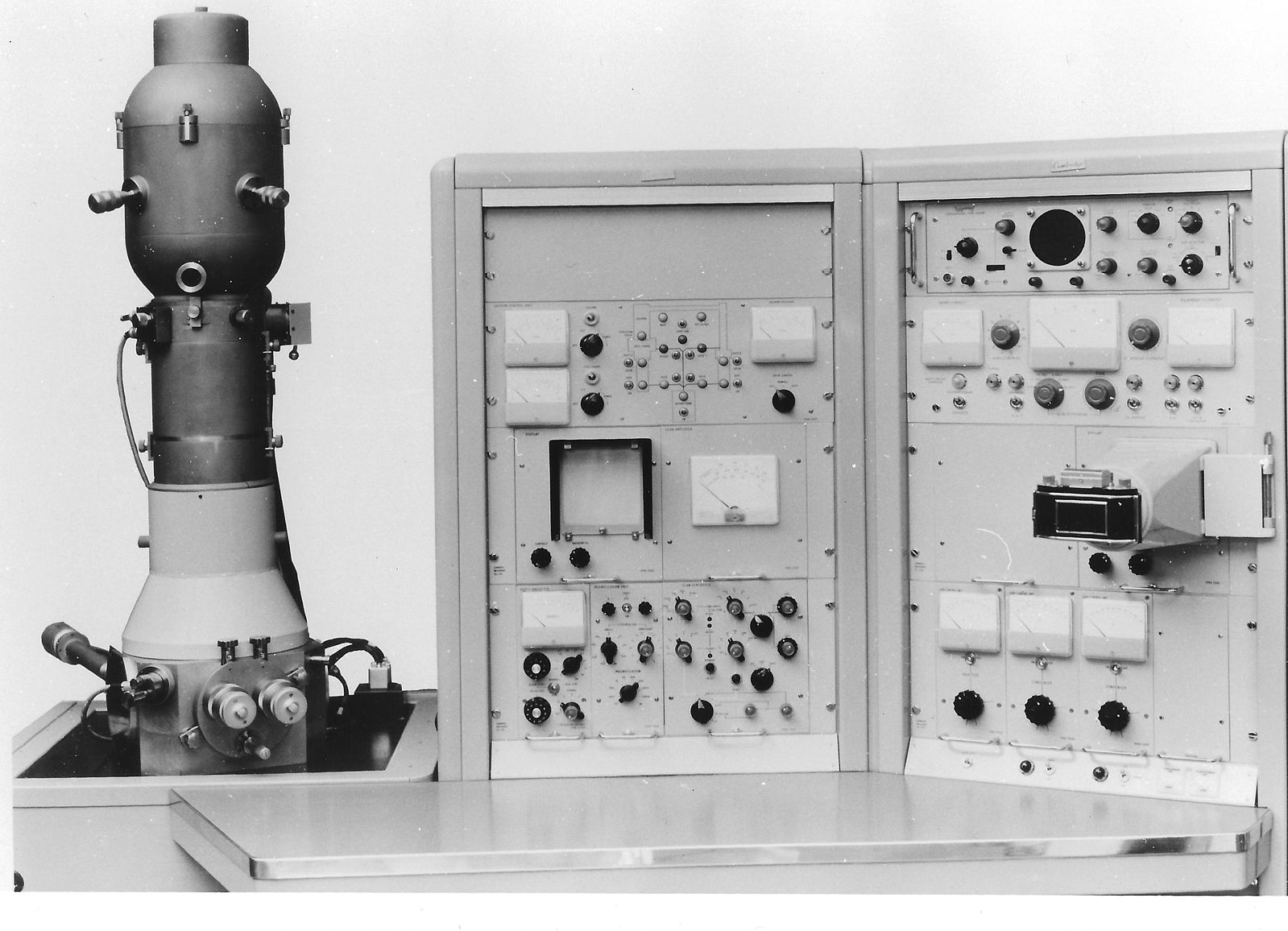
This instrument laid the groundwork for the modern Scanning Electron Microscope, marking a significant milestone in the field of microscopy. SEM's ability to produce three-dimensional images of a specimen's surface was a game-changer, making the Stereoscan a coveted tool in the scientific community.
SEM in the Modern Era: Continuous Innovation and Advancement
Today, continuous advancements in technology have greatly enhanced the performance and versatility of SEM. Improvements in resolution, depth of field, and electron detection technology have allowed SEMs to produce even more detailed and insightful images of specimens.
Technological innovations such as Field Emission SEM (FESEM), which uses a field emission gun to provide a smaller and more focused electron beam, and Environmental SEM (ESEM), which allows for the examination of hydrated samples, have expanded the application of SEM in various fields.
SEM's ability to link with other techniques, such as Energy-Dispersive X-ray Spectroscopy (EDS) and Electron Backscatter Diffraction (EBSD), have further enhanced its capabilities, making SEM an indispensable tool in numerous scientific explorations.
Electron Microscopy Techniques: Comparisons and Contrasts
While SEM has significantly contributed to the world of microscopy, it is one among several forms of electron microscopy techniques, each offering unique capabilities. Techniques such as Transmission Electron Microscopy (TEM), Reflection Electron Microscopy (REM), and Scanning Transmission Electron Microscopy (STEM) serve different purposes and suit varying research needs.
Transmission Electron Microscopy (TEM)
Unlike SEM, which scans the surface of the sample, TEM transmits a high-energy electron beam through an ultra-thin specimen. This technique provides information about the internal structure of the sample, revealing details at an atomic level. While TEM can offer a higher resolution than SEM, it requires a more complicated sample preparation process and lacks the three-dimensional imaging capabilities of SEM.
Reflection Electron Microscopy (REM)
REM uses low-energy electrons to investigate the surface structure and composition of samples. While it does not provide the depth of field or the three-dimensional imaging of SEM, REM can offer high-resolution images of a sample's surface.
Scanning Transmission Electron Microscopy (STEM)
STEM, a hybrid technique, combines elements of both SEM and TEM. It uses a focused beam of electrons scanned across a thin specimen, like in SEM, but it also collects transmitted electrons, as in TEM. STEM can provide both surface topography and internal structural information, offering a versatile approach for comprehensive sample analysis.
Each of these techniques, along with SEM, brings unique strengths to the table, emphasizing the diversity and adaptability of electron microscopy in answering a wide array of scientific inquiries.
Understanding the Functioning of Scanning Electron Microscopy
Understanding the workings of Scanning Electron Microscopy (SEM) can seem daunting, but think of it as using a highly advanced "magnifying glass" that uses electrons instead of light to "see" objects on a minuscule scale. This incredible tool is capable of revealing the secrets of the microscopic world around us.
How SEM Works: The Basic Principle
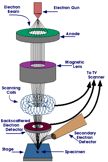
At its heart, SEM works in a somewhat similar way to a movie projector. However, instead of light, SEM uses a beam of high-energy electrons. This 'electron beam' is aimed at a sample we're interested in studying. When the beam hits the sample, it causes the release of other electrons and energy, creating signals that can tell us a lot about the sample.
These signals can give us valuable information about the sample's morphology (that is, its shape and size), its chemical composition (what elements it's made of), and its crystalline structure (how those elements are arranged).
What sets SEM apart from traditional light microscopy is its resolution and magnification. Light microscopes, like the ones you may have used in a school science class, use light waves to allow us to see small objects. However, they can only magnify an object up to about 2000 times its actual size. SEM, on the other hand, can magnify objects up to an impressive 1,000,000 times, enabling us to see objects that are much smaller than anything a light microscope could reveal.
The Parts of the SEM: What's Inside?
The SEM is composed of several key components that each play a critical role:
Electron Source or 'Gun': This is the source of the electron beam. It's like the film reel in our movie projector analogy.
Electron Lenses: These work like the lenses in a regular light microscope or a camera. They help focus the electron beam onto the sample.
Sample Stage: This is where the sample to be studied is placed. It can be moved around to aim the electron beam at different parts of the sample.
Detectors: These are like the movie screen in our analogy. They pick up the signals generated when the electron beam hits the sample and convert them into a picture.
In addition to these main parts, SEM requires a robust supporting infrastructure:
Power Supply: SEM needs a steady, strong source of power to operate.
Vacuum System: SEM works best in a vacuum, meaning all the air needs to be sucked out of the area where the sample is located.
Cooling System: The high-energy electron beam can generate a lot of heat, so SEM needs a cooling system to prevent overheating.
Vibration-free Floor and Room Free of Ambient Magnetic and Electric Fields: To get the best possible image, the SEM needs to be free of vibrations and external electromagnetic fields that might distort the electron beam.
By understanding how each part contributes to the functioning of an SEM, it's easier to appreciate the complexity and ingenuity behind this powerful tool.
Harnessing the Power of Scanning Electron Microscopy
Think of Scanning Electron Microscopy (SEM) as a 'super-microscope'. It can do a lot more than just make things look bigger. It has an array of unique abilities that enable scientists across a multitude of disciplines to explore the world on a microscopic scale, with an exceptional level of detail and precision.
SEM's Superior Capabilities: Magnification and Resolution
To truly appreciate the power of SEM, let's first understand its high magnification and resolution capabilities. Remember how SEM can magnify up to a million times? This means it can show us objects so tiny that they are invisible to the naked eye and even to many other types of microscopes.
Resolution, on the other hand, refers to how clear the image is. With high resolution, SEM can clearly distinguish between objects that are very close together. It's a bit like being able to tell apart two grains of sand on a beach - something you could never do with your naked eye or even with a light microscope.
The Power of Multi-Data Collection
What sets SEM apart is its ability to collect a variety of data all at once. Imagine if you could see an object, measure its temperature, and figure out what it's made of all in one go. That's the kind of information SEM can provide about a tiny sample.
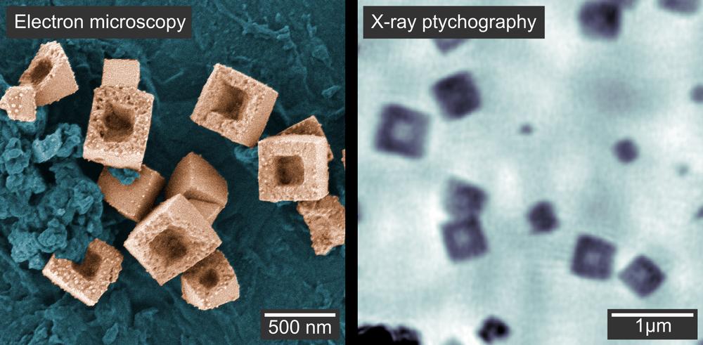
For example, SEM can show us the topography of a specimen, meaning it gives a detailed 'map' of the surface of the sample, showing all the 'hills' and 'valleys'. It also reveals the composition of the sample, telling us what elements it's made from. This is crucial information for many scientific disciplines.
SEM: A Versatile Tool for Numerous Fields
SEM is like a Swiss army knife for scientists, useful in a range of fields. Biologists use it to study things like bacteria, viruses, and cells. Geologists employ it to examine rocks and minerals. Material scientists find it invaluable for analyzing the structure of materials, from metals to ceramics. Even archaeologists use SEM to investigate ancient artifacts on a microscopic scale.
Enhancing SEM with Other Techniques
To make SEM even more powerful, scientists often combine it with other techniques. One such technique is Energy-Dispersive X-ray Spectroscopy (EDS). When the electron beam hits the sample, it can cause the release of X-rays. These X-rays can then be analyzed to determine the sample's elemental composition - a bit like revealing the 'ingredients' of the sample.
Another method is Backscattered Electron (BSE) imaging. Backscattered electrons are those that have bounced back after hitting the sample. By studying these, scientists can gain insights about differences in the atomic number (which is related to the element's weight) within the sample. It's a bit like being able to see which parts of a cake are chocolate and which are vanilla just by looking at it.
By harnessing the power of SEM and combining it with techniques like EDS and BSE, scientists are expanding the boundaries of our knowledge, discovering new things about our world on the tiniest scales.
Addressing the Limitations of Scanning Electron Microscopy
While Scanning Electron Microscopy (SEM) brings unparalleled benefits, it also presents several limitations. It's important to note these and understand how researchers are working tirelessly to overcome them to enhance SEM's functionality and scope.
High Vacuum Environment Requirement
SEM operations necessitate a high vacuum environment. This requirement is driven by the need to prevent the beam of high-energy electrons from colliding with air molecules, which could lead to the distortion of the resulting images. However, maintaining such a vacuum is challenging and calls for meticulous preparation and sample handling. Some samples may also respond poorly to vacuum conditions. Researchers have devised specialized preparation techniques to ensure sample stability and preservation under these conditions.
Conductivity and Size Constraints
The samples analyzed by SEM must be electrically conductive. Non-conductive specimens can accumulate charge from the electron beam, leading to image distortion. As a workaround, many biological samples, which are naturally non-conductive, are coated with a thin layer of conductive material, often gold, to ensure accurate imaging.
The SEM chamber's size also imposes limitations on the size of the samples that can be studied. Samples must not only fit within the chamber but also remain stable under vacuum conditions. Certain samples, due to their size or propensity to outgas under low pressure, are unsuitable for examination in conventional SEMs.
Investment and Training
Acquisition and maintenance of SEM equipment represent significant financial investments. Moreover, the operation of SEM equipment necessitates specialized training. Given the complexity and cost of these devices, their use is primarily limited to advanced research and industrial settings.
Overcoming the Limitations: Progress and Potential
Despite these limitations, progress in SEM technology continues at a swift pace. Developments in low vacuum and environmental SEMs have broadened the range of viable samples for analysis. Additionally, improvements in detector technology are enhancing SEM's ability to identify lighter elements and those with atomic numbers less than 11.
By consistently addressing these limitations, the scientific community is ensuring the continuous evolution of SEM, maximizing its potential as a tool for high-resolution examination of a wide variety of samples.
The Role of Scanning Electron Microscopy in Nanotechnology
As we delve into the concluding remarks of our exploration into Scanning Electron Microscopy (SEM), it is important to highlight its significance in one of the most promising fields of our era: nanotechnology. In the nanoworld, where dimensions are measured in billionths of a meter, SEM emerges as a central investigative tool, illuminating features that would otherwise remain unseen.
Nanotechnology is revolutionizing various domains, including materials science, medicine, electronics, and environmental protection. Its ability to manipulate matter at an atomic or molecular scale unlocks potential for unprecedented technological advances. SEM, with its high-resolution imaging capabilities, provides a pathway to visualize and understand these nano-scale structures.
The superior magnification, resolution, and depth of field offered by SEM make it an invaluable tool in nanotechnology research. The nano-scale objects, once invisible to the human eye and inaccessible to traditional microscopy, can now be visualized in impressive detail using SEM. The intricate designs of nanomaterials, the novel structures of nanoparticles, and the complex arrangements of nanodevices – all are laid bare under the scrutiny of SEM.
Furthermore, SEM offers more than just visualization; it provides vital analytical data. By incorporating techniques such as Energy-Dispersive X-ray Spectroscopy (EDS) and Backscattered Electron (BSE) imaging, SEM can reveal elemental composition and crystalline structure of nanomaterials. This ability to not just see but also understand the materials at a nano-scale aids in the design and synthesis of new nanomaterials and devices.
However, as we've discussed previously, SEM is not without limitations. The necessity for vacuum conditions, the need for samples to be conductive, and constraints on the size of samples are all challenges in nanotechnology applications. Yet, ongoing improvements in SEM technology, such as advancements in low-vacuum and environmental SEMs, are helping overcome these barriers, extending SEM's reach in the field of nanotechnology.
Frequently Asked Questions (FAQs) about Scanning Electron Microscopy (SEM)
What is Scanning Electron Microscopy (SEM)?
Scanning Electron Microscopy (SEM) is a type of electron microscopy that uses a focused beam of high-energy electrons to generate detailed images of the surface of solid specimens. These images can provide valuable information about a sample's external morphology, chemical composition, and crystalline structure.
How does SEM work?
SEM operates by projecting a focused beam of high-energy electrons onto the surface of a solid sample. When these electrons hit the sample, they interact with its atoms, causing various signals to be emitted. These signals can be captured and used to generate a highly detailed image of the sample's surface.
What are the main components of an SEM?
The primary components of an SEM include the Electron Source or 'Gun', Electron Lenses, Sample Stage, and Detectors for each signal of interest. It also requires an infrastructure consisting of a robust Power Supply, Vacuum System, Cooling system, a vibration-free floor, and a room free of ambient magnetic and electric fields.
What are the main applications of SEM?
SEM is an essential tool in many scientific fields, including biology, geology, materials science, and archaeology. It's used to generate high-resolution images of objects' shapes, to show spatial variations in chemical compositions, and to examine the elemental composition of specimens when combined with other techniques like Energy-Dispersive X-ray Spectroscopy (EDS) or Backscattered Electron (BSE) imaging.
What are the limitations of SEM?
While SEM is a highly valuable tool, it has limitations. These include the need for a high vacuum environment, the requirement for samples to be electrically conductive, and size constraints of the SEM chamber. Additionally, SEM instruments are expensive and require specialized training to operate.
