Understanding Band Gap Engineering in Nanotechnology
Definition: Band Gap Engineering is a process used in semiconductor material science to tailor the energy gap between the valence and conduction bands. This manipulation affects how electrons and holes move within a material, impacting its electrical and optical properties. This article explores the concept, techniques, significance, and applications of Band Gap Engineering, especially in the context of nanotechnology.
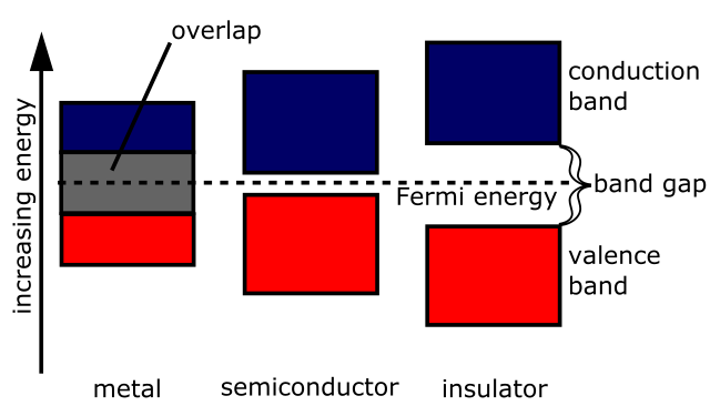
What is Band Gap Engineering?
At the heart of semiconductor physics, the band gap is a fundamental energy difference preventing electrons in the valence band from moving freely to the conduction band. Band Gap Engineering involves the intentional alteration of this gap to customize the material's electronic and optical behaviors for specific applications.
Techniques and Methods
Techniques for Band Gap Engineering vary, including doping, the introduction of impurities into a semiconductor to alter its electrical properties; strain engineering, where stress is applied to modify the semiconductor's crystal lattice; and quantum well creation, involving thin layers of semiconductors sandwiched between barriers to confine electron motion. Additionally, nanostructuring—altering the material's structure at the nanoscale—has emerged as a powerful method to engineer band gaps.
Significance in Nanotechnology
In nanotechnology, Band Gap Engineering is pivotal for developing advanced materials with tailored electronic, optical, and magnetic properties. By controlling the band gap at the nanoscale, scientists can create highly efficient semiconductors, photovoltaic cells, and light-emitting diodes (LEDs), among other devices.
Applications
- Photovoltaics: Engineered band gaps enable the development of solar cells that more efficiently convert sunlight into electricity by absorbing a broader spectrum of light.
- LEDs: Adjusting the band gap of materials used in LEDs can produce light of different colors, enhancing their use in displays and lighting technologies.
- Transistors: Semiconductor devices benefit from Band Gap Engineering by achieving better on/off switching behaviors, critical for computer chips and electronic devices.
- Sensors: Tailored band gaps improve the sensitivity and selectivity of sensors for environmental monitoring, healthcare, and industrial applications.
Challenges and Future Directions
Despite its potential, Band Gap Engineering faces challenges, including material stability and the complexity of nanoscale fabrication techniques. Future research is focused on overcoming these hurdles and exploring new materials and methods for more efficient and sustainable technological solutions.
Band Gap Engineering represents a cornerstone of modern materials science, enabling the precise control of semiconductor properties for innovative applications. As the field evolves, its contributions to technology and society are expected to grow, highlighting the importance of continued research and development in this area.
Further Reading
npj 2D Materials and Applications, Bandgap engineering of two-dimensional semiconductor materials
Coordination Chemistry Reviews, Band gap engineering of metal-organic frameworks for solar fuel productions
