Kelvin Probe Force Microscopy Explained: Nanoscale Surface Analysis
Definition: Kelvin Probe Force Microscopy (KPFM), also known as Surface Potential Microscopy, is a cutting-edge scanning probe microscopy technique that measures the surface potential of materials at the nanoscale. By providing detailed insights into the electrical properties of surfaces, KPFM plays a crucial role in the fields of material science, nanotechnology, and semiconductor research. This guide explores the fundamentals, operation principles, advantages, limitations, and applications of KPFM, tailored for those with a keen interest but no prior background in the subject.
Definition and Principle of Operation
KPFM is based on the principle of detecting the contact potential difference (CPD) between a conductive AFM tip and the sample surface. This difference is directly related to the work function difference between the tip and the sample. By nullifying this potential difference through an external applied bias, KPFM can measure the local surface potential with high spatial resolution.
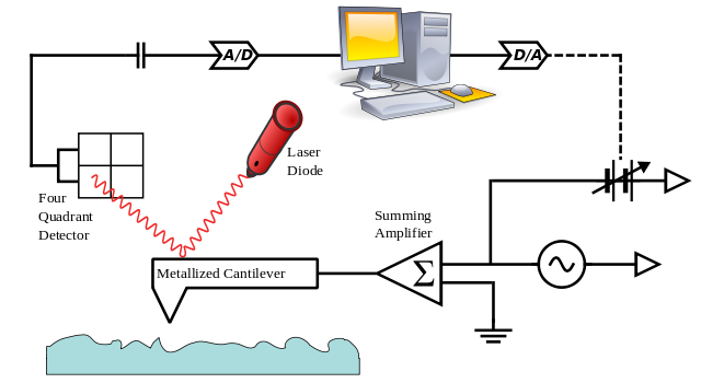
How Kelvin Probe Force Microscopy Works
The operational mechanism of KPFM involves oscillating the AFM tip near the sample surface without making physical contact. An AC voltage is applied to the tip, inducing an oscillation in the electrostatic force between the tip and the sample. A feedback circuit then adjusts a DC bias to the tip to minimize this force. The magnitude of the DC bias required to nullify the force oscillation is equal to the CPD, providing a measure of the sample's surface potential.
Key Features of Kelvin Probe Force Microscopy
KPFM offers several distinctive advantages:
- Non-Destructive Measurement: Like its parent technology AFM, KPFM is non-contact and non-destructive, allowing for the analysis of sensitive materials without damage.
- High Spatial Resolution: KPFM can achieve nanometer-scale resolution, enabling detailed visualization of surface potential variations at the nanoscale.
- Quantitative Analysis: It provides quantitative measurements of the surface work function and potential, which are crucial for understanding material properties.
- Versatility: KPFM can be applied to a wide range of materials, including conductors, semiconductors, and insulators.
Limitations of Kelvin Probe Force Microscopy
However, KPFM also faces some challenges:
- Surface Sensitivity: Measurements can be influenced by surface contamination, requiring strict sample preparation and handling protocols.
- Environmental Sensitivity: Atmospheric conditions and humidity can affect measurements, often necessitating controlled environments for accurate data.
- Complex Data Interpretation: The interpretation of KPFM data can be complex, requiring a thorough understanding of the technique and the sample's properties.
Applications of Kelvin Probe Force Microscopy
KPFM's applications span numerous fields, showcasing its versatility:
- Material Science: It is used for investigating surface chemistry and composition, and mapping work function variations across different materials. For example, KPFM can distinguish between different phases in a multi-phase polymer blend, revealing how each phase contributes to the material's overall electrical properties.
- Semiconductor Research: In semiconductor research, KPFM characterizes semiconductor devices, measures dopant distributions, and identifies defects. For instance, it can map the potential distribution across a semiconductor junction, providing insights into the efficiency and performance of electronic devices.
- Nanotechnology: KPFM studies charge distribution in nanostructures and devices, advancing understanding of nanoscale electrical phenomena. For example, it can assess the charge storage capability of nanoscale memory devices, aiding in the design of more efficient data storage technologies.
- Photovoltaics: In photovoltaics, KPFM helps scientists analyze the electrical properties of solar cell materials and interfaces to improve energy conversion efficiency. For instance, it can identify potential barriers at the interfaces of different layers within a solar cell, which are critical for optimizing device performance.
- Corrosion Science: KPFM assesses the protective quality of coatings and the corrosion potential of metals and alloys. For example, it can evaluate the effectiveness of corrosion inhibitors on metal surfaces, providing valuable information for the development of more durable materials.
Recent Technological Advancements in Kelvin Probe Force Microscopy
Recent advancements in KPFM include the development of high-speed scanning capabilities and the integration with other spectroscopic techniques, broadening its application scope. Innovations in probe design and feedback mechanisms have significantly enhanced resolution and sensitivity, allowing for more detailed and accurate surface potential measurements.
Environmental and Biological Applications
In environmental science, KPFM assists in the study of atmospheric particles and pollutants. In biology, it enables the mapping of electrical properties in biological membranes and cells, contributing to our understanding of bioelectrical phenomena.
Art and Cultural Heritage Conservation
KPFM is also making inroads into the conservation of art and cultural heritage, where it helps in the diagnosis of degradation mechanisms in historical artifacts by assessing their surface electrical properties.
Further Reading
Surface Science Reports, Kelvin probe force microscopy and its application
