| Posted: Jun 03, 2014 |
Prototype of new transistor for lower power consumption
|
|
(Nanowerk News) Researchers from the University of Twente MESA+ research institute, together with the company SolMateS, have developed a new type of transistor to reduce the power consumption of microchips. The basic element of modern electronics, namely the transistor, suffers from significant current leakage. By enveloping a transistor with a shell of piezoelectric material, which distorts when voltage is applied, researchers were able to reduce this leakage by a factor of five (compared to a transistor without this material). An article presenting the prototype of the transistor appears in the June issue of Transactions on Electron Devices ("Integration of a Piezoelectric Layer on Si FinFETs for Tunable Strained Device Applications"), an authoritative scientific journal in the field of transistor research.
|
|
Current leakage in transistors is one of the causes of battery depletion in portable electronic devices, such as smartphones and laptops. With the new type of transistor, either the current leakage (while the transistor is not active) or the energy consumption (while the transistor is active) can be addressed. In the latter case, it is estimated that energy consumption can be reduced by approximately 10%.
|
|
Intelligent squeezing
|
|
The trick lies in a piezoelectric material which is applied to the exterior of the transistor. The piezoelectric material expands when you apply a voltage to it and compresses the silicon in the transistor with a pressure of about 10,000 atmospheres. This high pressure ensures that electrons flow through the transistor faster. You can therefore make microchips more efficient by 'intelligently squeezing the transistor'.
|
|
Incidentally, existing transistors are already put under high pressure in order to improve their efficiency. In this case, however, the pressure is permanently built in, which actually increases the current leakage. In the prototype designed by the UT, the transistor is only put under pressure when required and this makes a big difference. The electric current needed to switch the transistor from on to off is thereby partly replaced by mechanical tension.
|
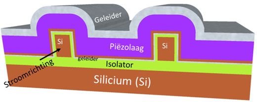 |
| Sketch of the transistor prototype. The transistor current flows through tiny silicon bars, which are enveloped by a package of conductor layers and piezo-electric material. The conductors control the amount of mechanical tension, and also the quantity of electrons in the silicon. In this way, the power can be turned on and off.
|
|
Crude
|
|
According to dr. ir. Ray Hueting from the chair Semiconductor Components, this is an initial prototype that can already produce energy savings. "The design is still fairly crude where the material is concerned. With the further development of the transistor, it should therefore be possible to achieve a further significant increase in efficiency."
|
|
The operating principle of this transistor was theoretically predicted in 2013 by the same research group. But in advance it was by no means certain that the transistor would be a success. The reason for this is that piezoelectric materials and silicon (which transistors are made of) are difficult to combine. The researchers solved this by inserting a buffer layer between the two materials.
|
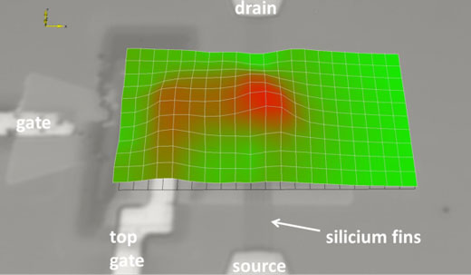 |
| Top view of the upward movement of a piezo FET with 5 parallel silicon bars (also referred to as 'fins') as a result of the piezo-electric effect. When an electrical current is applied across the piezoelectric material, the green parts do not move, but the red ones do.
|
|
Research
|
|
The research was performed by Buket Kaleli, Ray Hueting and Rob Wolters from the University of Twente. Staff from SolMateS, a University of Twente spin-off company, applied the piezoelectric layer to the transistor. The research was financially supported by the Technology Foundation STW.
|

