| Posted: Jun 18, 2014 |
Energy-level alignment at metal/organic interfaces: Tying up the loose ends |
| (Nanowerk News) Organic semiconductors have tremendous potential for complementing conventional, inorganic semiconductors as active materials in (opto-)electronic devices such as light-emitting diodes (OLEDs) for display and lighting applications or solar cells (OPVCs). Electrical connection of such devices to peripheral circuitry, however, is realized by metallic contacts and the resulting interfaces to the organic semiconductor have been found to play a central role: Energy barriers for injecting charge carriers into the organic (OLEDs) or energy losses upon their extraction (OPVCs) were found to detrimentally affect device performance. |
| Attempts to minimize these energy barriers/losses are hampered by an incomplete understanding of their origin and the parameters that govern their magnitude. A multitude of sometimes conflicting views have been expressed in literature, each treating only a certain limiting case under particular assumptions for interface properties and dominant mechanism. |
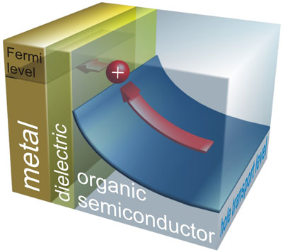 |
| When inserting an ultrathin dielectric between metal electrode and organic semiconductor, charge carriers (shown here for a positively charged holes in red) are, counter intuitively, more efficiently extracted from their transport level (blue) in the organic to the Fermi level (black) in the metal than without the interlayer. (Image: M Oehzelt/HZB) |
| Now, a team including IRIS-member Norbert Koch implemented a detailed electrostatic model ("Organic semiconductor density of states controls the energy level alignment at electrode interfaces"), which is capable of covering the full phenomenological range of interfacial energy-level alignment regimes within a single, consistent framework. Energy barriers/losses could be reproduced in both qualitative and quantitative agreement with a series of experiments. By continuously connecting the limiting cases described by previously proposed models, conflicting views in literature could be resolved. |
| In particular, the team highlighted the key role played by the density of electronic states in the organic semiconductor: Its shape was found to determine both the minimum value of practically achievable injection barriers as well as their spatial profile, ranging from abrupt steps at the interface with the electrode to smoothly varying curves. Especially the latter – counter intuitively induced by introducing an ultrathin, electrically insulating interlayer between metal and organic – is beneficial for charge extraction in OPVCs, as illustrated above. |
| Source: Helmholtz Zentrum Berlin |

