| Posted: Jun 25, 2014 |
Waveguiding and detecting structure for surface plasmon polaritons on silicon |
| (Nanowerk News) Surface plasmon polaritons (SPPs) are waves that propagate along the surface of a conductor and collective oscillation of electrons coupled with the optical field at the nano-scale beyond the diffraction limit of propagating light waves. Recently, there is increasing interest in SPPs as signal carriers in nanoscale integrated circuits to increase the degree of accumulation and reduce power consumption. |
| However, low-loss SPP waveguides with detectors have not been developed for applying to nanoscale integrated circuits. |
| Now, Mitsuo Fukuda and his group at Toyohashi Tech have developed a simple, low-loss waveguide for SPPs that is applicable to nanoscale integrated circuits ("Low-loss waveguiding and detecting structure for surface plasmon polaritons"). |
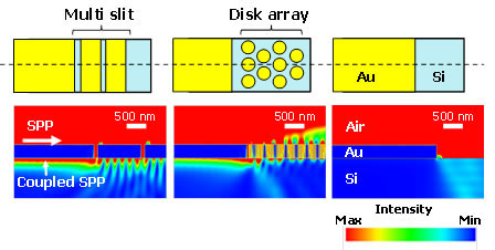 |
| Schematic diagrams and electric field intensity distributions for (a) a multi-slit structure, (b) a disk array, and (c) no diffraction structure at the waveguide end. |
| A thin metal film deposited on a silicon substrate was terminated with a diffraction structure (a multi-slit or a metal disk array) at the end to guide the SPPs transmitted on the surface (air-metal interface) to the opposite side of the metal (metal-silicon interface). A Schottky barrier is formed at the metal- silicon interface, and the free electrons in the metal are excited by the guided SPPs and then cross over the barrier. The overflowing electrons result in observable photocurrents. |
| The waveguide developed in this research enabled the efficient propagation of SSPs in 1550-nm-wavelength bands (transparent to silicon) along the Au film surface, and the photocurrents were much larger than for waveguides without the diffraction structure (26 times for the grating structure and 10 times for the disk array). |
| This waveguide device is expected to contribute to nanoscale photonic integrated circuits on silicon. |
| Source: Toyohashi University |

