| Posted: Jul 11, 2014 |
A summary of the state-of-the-art knowledge about graphene grain boundaries |
| (Nanowerk News) Graphene has attracted overwhelming attention both for exploring fundamental science and for a wide range of technological applications. Chemical vapor deposition (CVD) is currently the only working approach to grow high-quality graphene at very large scale, which is required for industrial applications such as high-frequency devices, sensors, transparent electrodes, etc. Unfortunately, the produced graphene is typically polycrystalline, consisting of a patchwork of grains with various orientations and sizes, joined by grain boundaries of irregular shapes. The understanding of the relation between polycrystalline morphology and charge transport is crucial for the development of applications, as recently reported by SAMSUNG. |
| Researchers from the ICN2 Theoretical and Computational Nanoscience Group curated a review article in Advanced Materials ("Charge Transport in Polycrystalline Graphene: Challenges and Opportunities") to determine whether graphene grain boundaries are a blessing or a curse. ICREA Research Professor Stephan Roche, Group Leader at ICN2, together with Dr Aron Cummings, Jose Eduardo Barrios Vargas and Van Tuan Dinh, from the same Group, share the authorship of the review with researchers from Sungkyunkwan University. The review article not only provides guidelines for the improvement of graphene devices, but also opens a new research area of engineering graphene grain boundaries for highly sensitive electro-biochemical devices. |
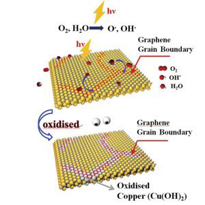 |
| The review analyses the challenges and opportunities of charge transport in polycrystalline graphene, which means summarizing the state-of-the-art knowledge about graphene grain boundaries (GGBs). The review is divided in the following sections: Structure and Morphology of GGBs; Methods of Observing GGBs; Measurement of Electrical Transport across GGBs; Manipulation of GGBs with Functional Groups. |
| The work describes how TEM and STM, combined with theory and simulation, can provide information for the observation and characterization of GGBs at the atomic scale. These boundaries have interesting properties, such as the fact that they can be a good template for the synthesis of 1D materials, might be useful to design sensors for detecting gases and molecules or allow selective diffusion of limited gases and molecules. Controlling the atomic structure of GGBs by CVD is a big challenge from a scientific point of view, but would be a huge step forward in the realization of next-generation technologies based on this material. |
| The work has been partly funded by SAMSUNG within the Global Innovation program. |
| Source: Catalan Institute of Nanoscience and Nanotechnology |

