| Posted: Aug 28, 2014 |
Materials other than silicon for next generation electronic devices
|
|
(Nanowerk News) In the consumer electronics industry, the mantra for innovation is higher device performance/less power. Arun Thathachary, a Ph.D. student in Penn State's Electrical Engineering Department, spends his days and sometimes nights in the cleanroom of the Materials Research Institute's Nanofabrication Laboratory trying to make innovative transistor devices out of materials other than the standard semiconductor silicon that will allow higher performance using less power.
|
|
Silicon has been the most successful material of the 20th century, with major global industries and even a valley named after it. But silicon may be running out of steam for high performance/low power electronics. For example, the compound semiconductor indium gallium arsenide is known to have far superior electron mobility than silicon. As silicon strains against the physical limits of performance, could a material like InGaAs provide enough of an improvement over silicon that it would be worth the expense in new equipment lines and training to make the switch worthwhile? Samsung, one of the world's largest electronics companies, has funded Thathachary through his adviser, professor of electrical engineering Suman Datta, in a project to help them find out.
|
|
In an article in the journal Nano Letters early this year ("Electron Transport in Multigate InxGa1–xAs Nanowire FETs: From Diffusive to Ballistic Regimes at Room Temperature"), Thathachary and his coauthors described a novel device prototype designed to test nanowires made of compound semiconductors such as InGaAs. Their goal was to see for the first time if such a compound material would retain its superior electron mobility at nanoscale dimensions in a so-called FinFET device configuration, the standard transistor architecture for sub-22 nanometer technology.
|
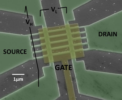 |
| Scanning Electron Microscope micrograph of multigate InGaAs nanowire field effect transistor with an array of five nanowires of width 40 nm. (Image: Arun Thathachary, Penn State)
|
|
"We developed a novel test structure called a Multi-fin Hall Bar Structure. It is the first such measurement of Hall mobility in a multi-fin 3D device," Thathachary said. "If you look at mainstream chip production today, all transistors are made in a 3D fashion, and because they are made in 3D rather than the earlier planar design, several mechanisms can degrade performance. What we looked at in that paper is how much degradation do you really suffer when going from a planar 2D surface to, in this case, 30 nm size features that are confined in 3D?"
|
|
What Thathachary and colleagues discovered was that electron mobility declined in a regular slope and that the experimental results could be modeled by a method called scattering relaxation time approximation. Using this technique they were able to predict how a compound semiconductor device would be likely to operate at the size at which this material would possibly be adopted, for example, the 7 nm technology node.
|
|
"We found that at dimensions of even 5 nm, you can still expect a 2x to 3x advantage in the mobility of these materials over silicon, which is very significant," said Thathachary. "After we published this paper, it was clear from a fundamental physics point of view that if you engineer the device correctly you should outperform existing silicon devices. But will it really? That's what we set out to investigate next."
|
|
Conference paper draws interest
|
|
The VLSI Symposia is an international conference on semiconductor technology and circuits, the leading conference for discussing advances in microelectronic devices. The majority of the presenters are from industry, with only a handful of student papers picked for presentation. At this year's VLSI, one of the papers was Thathachary's.
|
|
"The paper in Nano Letters was a precursor to the one chosen for the conference," Thathachary said. They had made a device with 30 nm features and measured the compound semiconductor's electron mobility down to that scale, but now it was time to actually make nanoscale transistors out of the new materials system and understand transistor behavior in that system.
|
|
Two of the parameters that are most important in transistor technology are called "subthreshold slope" and the "on current." Subthreshold slope indicates how efficiently you can turn the transistor on and off. While on current simply means how much current you can get out of the device. Especially for mobile devices, if the transistor can get the same amount of current with lower voltage it will extend battery life and reduce the amount of heat that has to be gotten rid of.
|
|
"In addition, it's imperative that you increase the functionality of the computer chip," Thathachary explained, "but that means putting more transistors inside. If you are going to put a 50 or 60 watt limit on the average power consumption of your chip, then those transistors have to require lower power than the existing devices."
|
|
Working on his Ph.D. project and through regular consultation with the Penn State Nanofab engineering staff, Thathachary spent a year in the cleanroom optimizing the processes required to put a new material system into a state of the art 3D FinFET device. That required spending many hours tweaking the conditions, such as temperature, flow rate, types of reactant gases, as well as refining his electron beam lithography and dry etch patterning techniques.
|
|
One of the most challenging issues he overcame was etching InGaAs into dense fin arrays comprising nanoscale dimensions. Once that was accomplished, he then needed to see how the new compound semiconductor system interacted with the other materials systems, such as the high-k dielectric thin film coating that surrounded the InGaAs fin.
|
|
"If you can get that process right, then you can make a great device, and that is what we showed at the conference," he said. "We showed that in terms of on current at lower supply voltage we are seeing very good performance compared to existing silicon devices."
|
|
Between the time the conference paper was accepted and the June meeting in Hawaii, Thathachary had continued to refine his processes. He learned that increasing the percentage of indium in the ternary (3-part) material system increased electron mobility significantly. Another mobility boost comes from engineering the dimensions of the active material so that the electrons are forced toward the middle of the material in a process called quantum confinement. This is important because in traditional transistors the electrons move close to the surface where they are exposed to microscopic roughness that degrades their mobility.
|
|
"The paper was remarkably well received at the conference, and we had a lot of requests to share our new and improved results. We had to get permission from Samsung to share that material, and eventually we did," Thathachary said.
|
|
Encouraged by his results, Samsung has since renewed the contract with the Datta lab and Thathachary for another year. His next challenge will be the most difficult so far. They want him to investigate the performance of a 3D transistor at the 7 nm dimension, a node that the semiconductor industry is looking at for the future. To do this in the Penn State Nanofab for the first time, means he will need to develop innovative ideas to overcome the limitations of working with limited resources in a university lab. Once a device can be made at or approaching those dimensions, Samsung will likely internalize the research and assign a large team of engineers to develop reproducible industry scale devices.
|
|
"If we can show that at those dimensions, these III-V compound semiconductor systems can still beat silicon, that is when it makes sense for industry to move in and invest the billions of dollars required for the new technology generation," Thathachary concluded.
|

