| Posted: Sep 24, 2014 |
Charge transport jamming in solar cells |
| (Nanowerk News) Researchers from the Max Planck Institute for Polymer Research in Mainz, jointly with scientists from Switzerland and Spain, have investigated the working mechanism of a new type of solar cells in which an organic-inorganic perovskite compound forms the light-absorbing layer. These cells can be produced in an inexpensive way with the simplest means. In comparison, the conventional silicon solar cells are energy-intensive and expensive to manufacture. Using Kelvin probe microscopy, the team of Mainz researchers around Rüdiger Berger and Stefan Weber observed the charge transport inside an illuminated solar cell. They found out that the positively charged carriers accumulated in a particular region in the solar cell. This phenomenon could be compared to a bottleneck on a freeway: should many cars – or charge carriers in our case – want to pass the bottleneck at the same time, the traffic will inevitably slow down or come to a halt. |
| According to these findings, the perovskite solar cells could soon achieve efficiencies comparable to those of commercial solar cells. Their results are published in the scientific journal Nature Communications ("Real-space observation of unbalanced charge distribution inside a perovskite-sensitized solar cell"). |
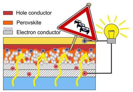 |
| Schematic of the working principle of a perovskite solar cell. (Illustration: S. Weber) |
| The perovskite solar cells produced in a laboratory directed by the Swiss scientist Michael Grätzel contain a layer of an organic-inorganic compound which crystallizes in the cubic perovskite structure. "These structures absorb light very well", says Rüdiger Berger explaining the working mechanism of these solar cells. "The light absorbed by the perovskite layer snatches an electron from an atom creating a positively charged electron vacancy - also known as "hole". Now the electrons just have to be brought to the electrode on the one side of the cell and the holes to the other side. That’s all we need for a working solar cell." |
| In the solar cell, the perovskite film therefore rests on a nanostructured layer of titanium dioxide that collects the electrons generated upon exposure to light and conducts them to the lower electrode. The holes are conducted to the upper electrode by a layer of the organic hole conductor material spiro-OMeTAD situated on top of the perovskite film. |
| "The many different layers in the solar cell are extremely important. They ensure an efficient sorting between the two charge carrier types" adds Berger's colleague Stefan Weber. "However, the charge carriers have to overcome a small barrier every time they jump from one material to the other. These barriers act like a construction site on a busy freeway where the vehicles clog. This charge transport jamming in the solar cell leads to losses and thus to a lower efficiency". |
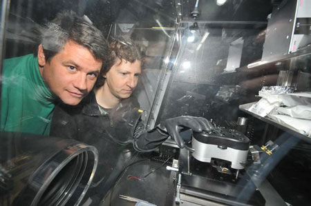 |
| Measuring a solar cell: Rüdiger Berger (left) and Stefan Weber (right). |
| In order to observe the charge transport within the solar cell, the Mainz researchers have split the cell in two halves. They then polished the cross section with a finely focused ion beam. With the fine tip of a scanning force microscope, they were able to image the structure of the layer down to a resolution of a few nanometers. In addition, Kelvin probe microscopy was contemporaneously used to measure the local electrical potential underneath the tip. From the potential distribution, the researchers were then able to derive the field distribution and thus the charge transport occurring through the various layers of the cell. |
| In several measurement series, the researchers found that a strong accumulation of positive charges takes place in the perovskite layer upon exposure to light. They suppose that titanium dioxide, the electron conductor, does its job much more efficiently than the hole conductor. In other words, the holes do not reach their electrode as fast as the electrons do; they accumulate along the way. The excess of positive charges in the perovskite layer results in the creation of a reversed electric field which also contributes to the slow down of the hole transport. |
| “We could for the first time correlate the charge distribution with the individual material layers in the cell”, says Rüdiger Berger. "The charge transport jamming of positive charges in the illuminated perovskite layer tells us that the transport through the hole conductor currently constitutes the bottleneck for the efficiency of the solar cell". The observations of the Mainz researchers can help to increase the efficiency of the perovskite solar cells over the 20% mark and thus offer a genuine alternative to the conventional silicon solar cells. |
| Source: Max-Planck-Institut für Polymerforschung |

