| Posted: Feb 17, 2015 |
Improving energy efficiency one atom at a time
|
|
(Nanowerk News) Paul Simmonds looks at his molecular beam epitaxy (MBE) system the way other guys do a candy apple red Porsche. The sci-fi looking machine used to design and create new materials at the atomic level lights his eyes with pure joy.
|
|
MBE is a cutting-edge technique that allows for the design and creation of completely new materials that don’t exist in nature. By creating extreme vacuum and temperature conditions, the instrument forces atoms to combine into unique nanoscale crystal layers. By adding additional layers of designer crystals, new materials can be created with specific or unusual properties.
|
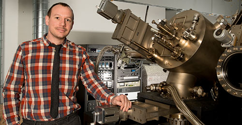 |
| Paul Simmonds at his molecular beam epitaxy (MBE) system.
|
|
Simmonds, a Cambridge graduate, came to Boise State in October from University of California, Los Angeles, where he managed the Integrated NanoMaterials Lab. Before that, he spent time as a post doc at Yale. He now is an assistant professor in both the Department of Physics and the Department of Materials Science and Engineering.
|
|
A key negotiation during the interview process was his ability to purchase an MBE system for his Boise State lab. While he didn’t get a brand spanking new model, which costs more than a million dollars, he did find one that had been used by the Air Force and affiliates and he has been refurbishing and customizing it in his lab in the Multipurpose Classroom Building.
|
|
While there still is a lot of work to be done to get it fully up and running, it will be a valuable new resource available to Boise State faculty and students and to industry members who want to collaborate with Simmonds in their research.
|
|
“MBE enables us to control the properties of new crystals with exquisite precision, right down to the atomic level,” Simmonds said. “We can grow nanomaterials with features just a few billionths of a meter across, and even control how many electrons they have inside them.”
|
|
In a nutshell, here’s how it works.
|
|
The machine is a bit like an atomic spray painter. Various “arms” are loaded with elements like germanium or aluminum, which are then beamed as atoms onto a substrate surface in a vacuum chamber. The atoms on the surface eventually sort themselves into a pattern, and continue to do so until a solid surface is formed. A new layer is then started and the process repeats itself until, sometimes many hours later, the final product is achieved.
|
|
“The strength of this is that it’s so versatile,” Simmonds said. “You can make all kinds of materials — metals, oxide materials, semiconductors …”
|
|
The process also controls for the purity of the material. There are faster methods, but they cannot compete with the material, quality, resolution and control offered by MBE.
|
|
Simmonds plans to build on previous research he did on a family of semiconductor nanostructures called III-V quantum dots. Quantum dots are useful for turning light into electricity, or electricity into light. His first project will use this technology to create a new kind of device to harvest waste heat and turn it into useful electricity. An example of waste heat would be a power station that loses a percentage of its heat energy generated by gas, coal or nuclear power.
|
|
“If we can capture this heat that is otherwise lost and turn it into electricity using our devices, then the overall efficiency of the power station goes up significantly,” he said. He is currently seeking grants to fund this line of research.
|
|
Simmonds said MBE systems are used in labs all over the world to push back the boundaries of physics, materials science, electrical engineering, chemistry and more.
|
|
“The number of things they can do is huge,” he said, “and they are highly interdisciplinary.”
|
|
The molecular beam epitaxy system is expected to be fully functional later this semester. To explore collaborating on a project using the MBE system, contact Simmonds at [email protected] or 426-3787.
|

