| Posted: Feb 20, 2015 |
Semiconductor works better when hitched to graphene |
| (Nanowerk News) Graphene – a one-atom-thick sheet of carbon with highly desirable electrical properties, flexibility and strength – shows great promise for future electronics, advanced solar cells, protective coatings and other uses, and combining it with other materials could extend its range even further. |
| Experiments at the Department of Energy’s SLAC National Accelerator Laboratory looked at the properties of materials that combine graphene with a common type of semiconducting polymer. They found that a thin film of the polymer transported electric charge even better when grown on a single layer of graphene than it does when placed on a thin layer of silicon (Advanced Functional Materials, "Enhanced Vertical Charge Transport in a Semiconducting P3HT Thin Film on Single Layer Graphene"). |
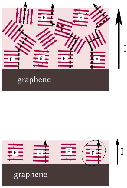 |
| Studies conducted at the Stanford Synchrotron Radiation Lightsource revealed that when deposited atop graphene, a thicker polymer film (top) conducted charge significantly better than a thinner polymer film (bottom). This is likely because the orientation of the polymer crystallites within the thick film allows the formation of a continuous pathway for the charge to flow. (Image: David Barbero) |
| “Our results are among the first to measure the charge transport in these materials in the vertical direction – the direction that charge travels in organic photovoltaic devices like solar cells or in light-emitting diodes,” said David Barbero of Umeå University in Sweden, leader of the international research team that performed the experiments at SLAC’s Stanford Synchrotron Radiation Lightsource (SSRL), a DOE Office of Science User Facility. “The result was somewhat expected, because graphene and silicon have different crystalline structures and electrical properties.” |
| But the team also discovered something very unexpected, he said. |
| Although it was widely believed that a thinner polymer film should enable electrons to travel faster and more efficiently than a thicker film, Barbero and his team discovered that a polymer film about 50 nanometers thick conducted charge about 50 times better when deposited on graphene than the same film about 10 nanometers thick. |
| The team concluded that the thicker film’s structure, which consists of a mosaic of crystallites oriented at different angles, likely forms a continuous pathway of interconnected crystals. This, they theorize, allows for easier charge transport than in a regular thin film, whose thin, plate-like crystal structures are oriented parallel to the graphene layer. |
| By better controlling the thickness and crystalline structure of the semiconducting film, it may be possible to design even more efficient graphene-based organic electronic devices. |
| “The fields most likely to benefit from this work are probably next-generation photovoltaic devices and flexible electronic devices,” said Barbero. “Because graphene is thin, lightweight and flexible, there are a number of potential applications.” |
| Source: SLAC National Accelerator Laboratory |

