| Posted: Apr 10, 2015 |
Electronic charge distribution on the atomic scale |
| (Nanowerk News) Scientists from the University of Göttingen and the Jülich Research Centre have made an important step towards a deeper understanding of metal-semiconductor interfaces. By means of a novel experimental approach the researchers investigated the distribution of the electronic charge at these interfaces on the atomic scale. Their results were published in the journal Physical Review Letters ("Local Density of States at Metal-Semiconductor Interfaces: An Atomic Scale Study"). |
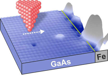 |
| Novel experiment on metal-semiconductor interfaces: A very sharp metal tip (red) is scanned across the iron/gallium arsenide interface. |
| In every electronic semiconductor device the interfaces between two different materials play a crucial role. In this context, the atomic and electronic structure of metal-semiconductor interfaces is of fundamental im-portance. For the development and the design of novel nanometer-sized devices, a basic understanding of these interfaces is of central interest. However, up until now, no commonly accepted model that describes metal-semiconductor interfaces in their entirety existed. This is also due to the fact that scientists did not have an adequate experimental approach to investigate the atomic structure of these interfaces. |
| Now scientists in Göttingen and Jülich investigated the technologically interesting iron/gallium arsenide inter-face using a scanning tunneling microscope developed in Göttingen. “By scanning a very sharp metal tip across the interface we were able to simultaneously map its structure and its electronic properties on the atomic scale,” explains doctoral candidate Tim Iffländer from Göttingen University’s IV. Physical Institute. “In combination with theoretical calculations from the colleagues in Jülich we found out that the electronic barrier between metal and semiconductor, on the one hand, is dominated by charges from the metal tailing into the semiconductor and, on the other hand, essentially depends on the chemical bonds between metal and semiconductor as well.” |
| “The high level of agreement between measured and calculated charge distribution at the interface demon-strates that our experimental approach is particularly well-suited to study the electronic properties of metal-semiconductor interfaces on the atomic scale,” adds Dr. Martin Wenderoth, head of the research group. “This allows us to check the relevance of several theoretical models. Moreover, our experiment serves as starting point for further studies addressing the influence of defects and the detailed atomic structure at the interface on the electronic properties of metal-semiconductor contacts.” |
| Source: Georg-August-Universität Göttingen |

