| Posted: Jun 24, 2015 |
Nanowires could be the LEDs of the future |
| (Nanowerk News) The latest research from the Niels Bohr Institute shows that LEDs made from nanowires will use less energy and provide better light. The researchers studied nanowires using X-ray microscopy and with this method they can pinpoint exactly how the nanowire should be designed to give the best properties. The results are published in the scientific journal, ACS Nano ("Fast Strain Mapping of Nanowire Light-Emitting Diodes Using Nanofocused X-ray Beams"). |
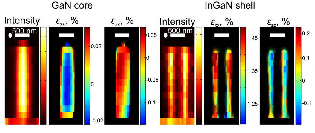 |
| The X-ray images of each nanowire show the distribution of the scattering intensity and the mechanical strain in the core of gallium-nitride and the shell of indium-gallium-nitride. The strain shows that the shell fits perfectly with the core. (Image: Tomas Stankevic, Niels Bohr Institute, University of Copenhagen) (click on image to enlarge) |
| Nanowires are very small - about 2 micrometers high (1 micrometer is a thousandth of a millimetre) and 10-500 nanometers in diameter (1 nanometer is a thousandth of a micrometer). Nanowires for LEDs are made up of an inner core of gallium nitride (GaN) and a layer of indium-gallium-nitride (InGaN) on the outside, both of which are semiconducting materials. |
| "The light in such a diode is dependent on the mechanical strain that exists between the two materials and the strain is very dependent on how the two layers are in contact with each other. We have examined a number of nanowires using X-ray microscopy and even though the nanowires should in principle be identical, we can see that they are different and have very different structure," explains Robert Feidenhans'l, professor and head of the Niels Bohr Institute at the University of Copenhagen. |
| Surprisingly efficient |
| The studies were performed using nanoscale X-ray microscopy in the electron synchrotron at DESY in Hamburg, Germany. The method is usually very time consuming and the results are often limited to very few or even a single study subject. But here researchers have managed to measure a series of upright nanowires all at once using a special design of a nanofocused X-ray without destroying the nanowires in the process. |
| "We measured 20 nanowires and when we saw the images, we were very surprised because you could clearly see the details of each nanowire. You can see the structure of both the inner core and the outer layer. If there are defects in the structure or if they are slightly bent, they do not function as well. So we can identify exactly which nanowires are the best and have the most efficient core/shell structure," explains Tomas Stankevic, a PhD student in the research group 'Neutron and X-ray Scattering' at the Niels Bohr Institute at the University of Copenhagen. |
| The nanowires are produced by a company in Sweden and this new information can be used to tweak the layer structure in the nanowires. Professor Robert Feidenhans'l explains that there is great potential in such nanowires. They will provide a more natural light in LEDs and they will use much less power. In addition, they could be used in smart phones, televisions and many forms of lighting. |
| The researchers expect that things could go very quickly and that they may already be in use within five years. |
| Source: University of Copenhagen |

