| Posted: Jul 09, 2015 |
Research alliance produces working test chips in 7-nm technology
|
|
(Nanowerk News) It’s an important moment in the history of the electronics industry. Researchers from IBM Research, SUNY Polytechnic Institute’s Colleges of Nanotech Science + Engineering and partners including GlobalFoundries and Samsung have produced advances that will enable the semiconductor industry to pack about twice as many transistors on the chips that power everything from data-crunching servers to mobile devices.
|
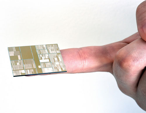 |
| Close up of the 7nm node test chip. (Photo: Darryl Bautista)
|
|
Working together, the team achieved an industry first–producing working test chips at New York’s SUNY NanoTech Complex near Albany whose smallest features approach 7 nanometers. As a result, the industry will be able to place more than 20 billion tiny switches on chips the size of a fingernail.
|
|
The implications of our achievement are huge for the computer industry. By making the chips inside computers more powerful and more efficient, IBM and our partners will be able to produce the next generations of servers and storage systems for cloud computing, big data analytics and cognitive computing.
|
|
With this feat by the alliance, we’re extending the life of the silicon semiconductor, one of the most important inventions of the 20th century, which has come to symbolize the seemingly inevitable march of technological progress–the ability to make all sorts of computers and electronic devices faster, smaller and more energy efficient. These advances represent the most significant chip-industry design and manufacturing innovations in nearly a decade.
|
|
In recent years, the chip industry has struggled to sustain a torrid pace of semiconductor innovation. Each wave of miniaturization has come only through near-superhuman feats of creativity by scientists and engineers.
|
|
IBM has played a critical role in many of these breakthroughs. For example, our scientists led the shift from aluminum wiring to copper to improve processing speeds; using Silicon on Insulator technology to reduce power consumption; and using High-k materials to reduce leakage of electrical current.
|
|
We achieved the latest step improvement, called the “7 nm node” by the chip industry, through a combination of new materials, tools and techniques. In materials, we’re using silicon germanium for the first time in the channels on the chips that conduct electricity. We have employed a new type of lithography in the chip-making process, Extreme Ultraviolet, or EUV, which delivers order-of-magnitude improvements over today’s mainstream optical lithography. All told, we’ve made dozens of design and tooling improvements. It has been a massive effort requiring multiple breakthroughs in science, technology and chip architectures and manufacturing processes.
|
 |
| 7nm node transistors packed below 30nm fin pitch. (Image: IBM Research)
|
|
Looking ahead, there’s no clear path to extend the life of the silicon semiconductor further into the future. The next major wave of progress, the 5 nm node, will be even more challenging than the 7 nm node has been.
|
|
IBM has committed to spending $3 billion on chip research and development aimed at further extending today’s mainstream semiconductor technologies even while we’re exploring innovations that depart radically from the use of silicon as a primary material in semiconductors and the use of transistors for processing data. We’re targeting new kinds of materials and technologies such as silicon photonics, carbon nanotubes and graphene; as well as entirely new approaches to computing, including neuromorphic computing and quantum computing.
|
|
Society is more than 50 years into the journey of silicon semiconductors, and, thanks to our work on the 7 nm node, the technology still has some runway. Now, we look further into the future and see the opportunity to reinvent computing. Science doesn’t get harder–or more satisfying–than this.
|

