| Posted: Jul 15, 2015 |
Scientists use large particle accelerator to visualize properties of nanoscale electronic materials
|
|
(Nanowerk News) A technique devised by UCLA researchers could help scientists better understand a tiny — but potentially important — component of next-generation electronic devices.
|
|
Scientists trying to improve the semiconductors that power our electronic devices have focused on a technology called spintronics as one especially promising area of research. Unlike conventional devices that use electrons’ charge to create power, spintronic devices use electrons’ spin. The technology is already used in computer hard drives and many other applications — and scientists believe it could eventually be used for quantum computers, a new generation of machines that use quantum mechanics to solve complex problems with extraordinary speed.
|
 |
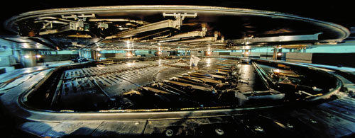
| UCLA researchers used the cyclotron at the TRI University Meson Facility, or TRIUMF, in Vancouver, British Columbia. (click on image to enlarge)
|
|
Emerging research has shown that one key to greatly improving performance in spintronics could be a class of materials called topological insulators. Unlike ordinary materials that are either insulators or conductors, topological insulators function as both simultaneously — on the inside, they are insulators but on their exteriors, they conduct electricity.
|
|
But topological insulators have certain defects that have so far limited their use in practical applications, and because they are so tiny, scientists have so far been unable to fully understand how the defects impact their functionality.
|
|
The UCLA researchers have overcome that challenge with a new method to visualize topological insulators at the nanoscale. An article highlighting the research, which was which led by Louis Bouchard, assistant professor of chemistry and biochemistry, and Dimitrios Koumoulis, a UCLA postdoctoral scholar, was published online in the Proceedings of the National Academy of Sciences ("Nanoscale β-nuclear magnetic resonance depth imaging of topological insulators").
|
|
The new method is the first use of beta-detected nuclear magnetic resonance to study the effects of these defects on the properties of topological insulators.
|
|
The technique involves aiming a highly focused stream of ions at the topological insulator. To generate that beam of ions, the researchers used a large particle accelerator called a cyclotron, which accelerates protons through a spiral path inside the machine and forces them to collide with a target made of the chemical element tantalum. This collision produces lithium-8 atoms, which are ionized and slowed down to a desired energy level before they are implanted in the topological insulators.
|
|
In beta-detected nuclear magnetic resonance, ions (in this case, the ionized lithium-8 atoms) of various energies are implanted in the material of interest (the topological insulator) to generate signals from the material’s layers of interest.
|
|
Bouchard said the method is particularly well suited for probing regions near the surfaces and interfaces of different materials.
|
|
In the UCLA research, the high sensitivity of the beta-detected nuclear magnetic resonance technique and its ability to probe materials allowed the scientists to “see” the impacts of the defects in the topological insulators by viewing the electronic and magnetic properties beneath the surface of the material.
|

