| Posted: Aug 26, 2015 |
More efficient chips based on plasmonics are a step closer(Nanowerk News) By using the tip of a scanning tunneling microscope (STM), A*STAR researchers and their collaborators have generated electromagnetic waves known as surface plasmon polaritons in a gold grating and demonstrated that the direction of travel of these waves can be controlled ("Electrically-excited surface plasmon polaritons with directionality control."). |
| This demonstration is a step toward the development of plasmonic chips, so called because they use plasmons — collective excitations of electrons in a conductor — rather than electrons to transfer and process data. Such chips promise to be much faster and potentially more energy efficient than current electronic chips. |
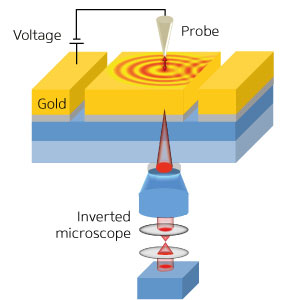 |
| Experimental setup used to investigate the directional excitation of surface plasmon polaritons in a one-dimensional gold grating. The probe of a scanning tunneling microscope is used to excite a surface plasmon polariton and the resulting light is analyzed by an inverted optical microscope. |
| Joel Yang and Zhaogang Dong at the A*STAR Institute of Materials Research and Engineering, together with colleagues at the A*STAR Institute of High Performance Computing and other institutes in Singapore, investigated controlling the traveling direction of plasmons in a gold grating both theoretically and experimentally. |
| In the experiments, they moved the STM tip relative to the edge of the gold grating and observed the generated light using an inverted microscope (see image).“The STM tip acts as a point source of surface plasmons,” Yang explains. “When placed on a metal film, electrons that tunnel across the gap can excite plasmons, although inefficiently.” |
| Yang likens the excitation of plasmons in gratings to dropping pebbles in a swimming pool with swimming lanes demarcated by floats. “What is interesting is that depending on how far we drop the pebble from the barrier for each lane, we can get waves that preferentially move away from the barrier and even across lanes. By adjusting the position just by a small amount — in our case by about 100 nanometers — we can turn on waves that propagate in the opposite direction, namely toward the barrier and beyond.” |
| This control of direction stems from the surface plasmon polariton reflected from the grating edge interfering with the one at the STM probe. By modeling this process on a computer, the researchers found a good match with the experimental results. |
| The result provides point sources of surface plasmon polaritons. This could prove useful for developing ways to replace wires between chips with optical connectors, which will greatly speed up chip-to-chip communication in integrated circuits based on plasmonics rather than electronics. |
| The researchers intend to investigate the optical characteristics of the plasmon source when the electrically excited plasmons are coupled to plasmonic waveguides, opening the way to plasmonic counterparts of electronic components. “Potentially, we hope to achieve logic gates, which underpin all processing circuits, based on electrically driven plasmons,” says Dong. |
| Source: A*STAR |

