| Posted: Oct 26, 2015 |
Thermoplastically deformable electronic circuits(Nanowerk News) At this week’s Meeting of the International Microelectronics Assembly and Packaging Society (IMAPS 2015), imec and CMST (imec’s associated lab at Ghent University) present a novel technology for thermoplastically deformable electronics enabling low-cost 2.5D free-form rigid electronic objects. The technology is under evaluation in Philips LED lamp carriers, a downlight luminaire and a omnidirectional lightsource, to demonstrate the potential of this technology in innovative lighting applications. |
| Thanks to its energy-efficiency, excellent light quality, and high output power, light emitting diode (LED) technology is becoming the sustainable light source for the 21st century. But in addition, it also allows to design unprecedented, innovative lighting solutions. Imec and CMST’s new thermoplastically deformable electronic circuits now add a new dimension to the possibilities to fabricate novel lamp designs as well as smart applications in ambient intelligence and wearables. |
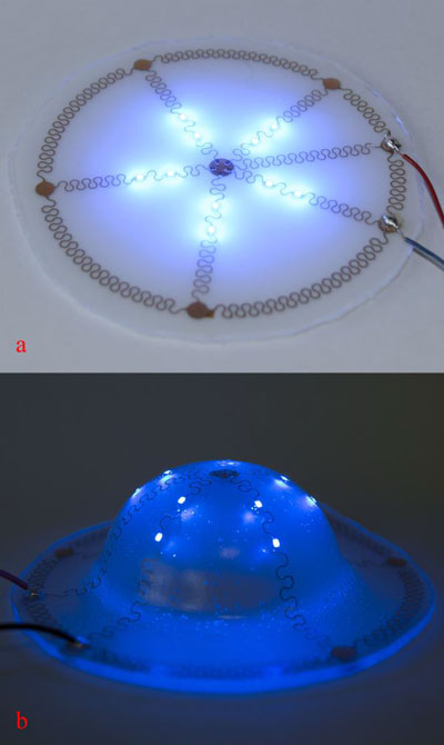 |
| Miniature LED dome test vehicle with integrated low power LEDs. (a) Device before forming. (b) Device after vacuum forming using a 40 mm half sphere. |
| The innovative technology is based on meander-shaped interconnects, a robust technique to realize dynamically stretchable elastic electronic circuits including LEDs. These are then embedded in thermoplastic polymers (e.g. polycarbonate). Following production on a flat substrate, using standard printed circuit board production equipment, the circuit is given its final form using thermoforming techniques such as vacuum forming, high pressure forming or even injection molding. Upon cooling, the thermoplastic retains its shape without inducing large internal stresses in the circuits. The method, based on standard available production processes, does not require large investments, reducing the cost of fabrication. The resulting designs have a low weight and low complexity, a high resilience, a low tooling and material cost, and a higher degree of manufacturer independence due to the standard industrial practices that are used. |
| The production process was developed in collaboration between the industrial and academic partners involved in the FP7 project TERASEL: imec, CMST (Ghent University), ACB, Holst Centre, Niebling Formtechnologie; Sintex NP and Philips Lighting BV. TERASEL is a European effort focusing on the development, industrial implementation and application of large-area, cost-effective, randomly shaped electronics and sensor circuit technologies. |
| Source: imec |

