| Posted: Dec 28, 2015 |
Simultaneous detection of the polarities of hundreds of semiconducting nanowires(Nanowerk News) Researchers at the University of Valencia have developed a technique to determine the individual polarities of hundreds of semiconducting nanowires in a single, time-saving process. Led by Ana Cros, director of the Universitat de València’s (UV) Materials Science Institute (ICMUV), the study constitutes a major step forward in both our understanding and application of these structures, since their polarity defines the properties of devices made from. |
| Semiconducting nanowires are structures just tens of nanometres in diameter with a typical length-to-width ratio of around 1000 – like a human hair, only a thousand times smaller. So much so that they are often referred to as one-dimensional materials, and indeed they have many interesting properties not seen in larger 3D materials. Semiconducting nanowires are currently among the most-studied nanometric structures and are the basic building blocks for a range of optoelectronic devices that source, detect and control light, such as light detectors, emittors and nanosensors. |
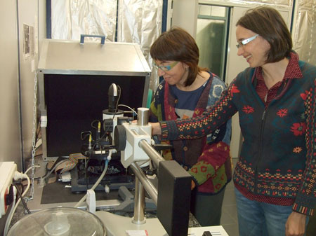 |
| Researchers Ana Cros and Nuria Garro. |
| Until now, determining their polarities required the nanowires to be analysed one-by-one as part of a complex and time-consuming process. This new technique uses an atomic-strength microscope and a Kelvin probe to detect minuscule forces and measure the electrical characteristics of the sample’s surface. When combined with advanced data analysis, these measurements reveal the polarities of hundreds of nanowires at the same time. |
| Ana Cros offers us an analogy: “Our microscope explores the surface of the sample in the same way that a blind person explores their surroundings: it uses a probe as a cane, getting an idea as to surface properties based on changes in vibrations. The difference between the microscope and the cane is that its point is extremely sharp. If we then add the electrical charge, we are able to measure the electrical characteristics of the surface of very small objects without even needing to touch them.” |
| Known as Kelvin probe force microscopy (KPFM), this technique has made it possible to determine the individual polarities of over 100 nanowires at the same time. Núria Garro, researcher at the ICMUV, explains: “What used to take days -having to select the nanowires one-by-one and ultimately destroying the sample- now takes a matter of hours, without incurring any damage whatsoever to the sample”. |
| The study was published in the journal Nano Letters ("Assessment of Polarity in GaN Self-Assembled Nanowires by Electrical Force Microscopy") and was carried out jointly with the University of Murcia, the University of Grenoble and the French Atomic Energy Commission. It constitutes one of the primary findings from a new line of researched opened at ICMUV for the study of optoelectronic processes in advanced materials and surfaces. It was carried out as part of the European project NANOWIRING (FP7-People) and was led in Valencia by Núria Garro. |
| Source: RUVID |

