| Posted: Jan 08, 2016 |
Legos for the fabrication of atomically precise electronic circuits(Nanowerk News) For the first time, researchers tailored the electronic properties of nanoribbons using a new “bottom-up” method that precisely controls and modulates the atomic-scale width within a single nanoribbon (Nature Nanotechnology, "Molecular bandgap engineering of bottom-up synthesized graphene nanoribbon heterojunction"). Simulations were used to further interpret how nanoribbons with non-uniform widths behave and confirmed that the modulated width altered the electronic properties as intended, specifically the bandgap that determines how electrons move through the material. |
| Unprecedented control over the shape and electronic properties at sub-nanometer scales allows atomic-level engineering of semiconductor heterojunctions with the potential for high-performance electrical circuits for faster, more energy efficient electronics and advanced solar cells. |
| Varying the width of tiny strips of graphene with atomic-scale precision is predicted to allow profound control over nanostructure electronic properties. This is analogous to a technique for modifying the electronic properties of electronic devices called “bandgap engineering.” |
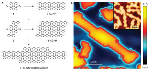 |
| The width of a graphene nanoribbon determines its electronic properties, but controlling that width at the atomic scale is a challenge. Graphene nanoribbon width has been controllably modulated within individual nanoribbons using molecular building blocks as shown in this scanning tunneling microscopy image. The lower magnification image (inset) shows multiple nanoribbons. |
| Bandgap engineering has been used in the past to create high-performance micron-scale devices from traditional semiconductors, but it remains an open question whether it can be scaled down to the molecular level. Conventional “top-down” fabrication methods are inadequate for this task because they lack the required spatial resolution. |
| For the first time, researchers led by the University of California at Berkeley and Lawrence Berkeley National Laboratory developed a new “bottom-up” approach that allows molecular bandgap engineering to be performed by controllably modulating the width of graphene nanoribbons at the atomic scale. Molecular building blocks were designed to fuse together to controllably modulate the width of a single nanoribbon in a series of connected segments, each having a different width specified at the atomic level. |
| Scanning tunneling microscopy (STM) was used to determine the shape of the nanoribbons and to spatially map how electrons arrange themselves within a single nanoribbon. Simulations were used to further interpret the STM images and to understand how nanoribbons with non-uniform widths behave. It was confirmed that the modulated width altered the nanoribbon electronic properties, specifically the bandgap that determines how electrons move through the material. |
| Modifying the bandgap within different nanometer scale segments along a single nanoribbon enables the creation of atomically engineered junctions. Such junctions within graphene nanoribbons could be used to produce high performance circuits for use in future electronics and solar cells. |
| Source: U.S. Department of Energy, Office of Science |

