| Posted: Feb 02, 2016 |
New method for producing tiny cracks in electrodes may mean big boost for nanoelectronics
(Nanowerk News) The next generation of electronics, as well as ultra-sensitive medical diagnostics, could depend on near atomic scale cracks — or nanogaps — in electrodes. Now, researchers at Sweden's KTH Royal Institute of Technology have developed a method that could pave the way for mass production of nanogap electrodes.
|
|
The researchers at KTH published a scalable method using nanocracks for creating nanogaps that are only a few atom layers wide (Advanced Materials, "Crack-Defined Electronic Nanogaps").
|
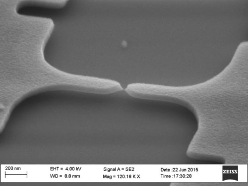 |
| A nanogap created with the new method. (Image: courtesy of KTH)
|
|
Valentin Dubois, a researcher at KTH's Department of Micro and Nanosystems, says the new method improves on established ways to achieve gaps in conductive materials — in this case, titanium nitride (TiN).
|
|
"Using our method, we do not need to pattern the material directly to define the nanogaps," Dubois says. "Instead, they arise automatically once certain criteria are met. What we need to do is create a pattern around the area where the gaps should be. This pattern in the material structure is substantially larger than the gaps, and thus simple to create."
|
|
The method, developed by Dubois and his research partners, Frank Niklaus and Göran Stemme, allows for mass production of nanogap arrays with individually-defined gap widths, he says.
|
|
What's more, for the first time, a method has been published that accurately predicts the cracks' characteristics. Dubois says that this enables one to determine at the outset what the parameters of the nanogaps will be, from 100 nm down to below 2 nm (less than ten atom layers) wide.
|
|
These nanometer-sized cracks in material with electrical conductivity can be used to study molecules' basic electrical properties, and how molecules interact with light.
|
|
"The ability to create nanogaps in a reliable and scalable manner will facilitate fundamental advances in molecular detection, plasmonics, and nanoelectronics," Dubois says.
|
|
Nanogaps could enable new types of microprocessors and make a whole range of biosensors possible. In medical diagnostics, for example, nanogaps can improve the detection of molecules that are markers for diseases. A light can be shined into the gaps of a material, enhancing the electromagnetic field within and allowing individual signals of a biomarker molecule caught in the gaps to stand out. The presence of such a molecule would be indicated by a change in the scattering of light.
|
|
Nanogaps can also be used with microprocessors, enabling them to become smaller and faster, and improving devices' energy efficiency and memory capacity, Dubois says.
|
|
Also, for medical purposes, nanogaps can be used as components of biosensors, such as those used for DNA sequencing, he says.
|
|
"Applications like these are traditionally in health care and medical research, but also for so-called wearable electronics, such as clothing with integrated electronics," he says.
|

