| Posted: Feb 02, 2016 |
Engineers finding uses for ultra-thin semiconductor lasers in medical, consumer fields
(Nanowerk News) A new type of ultra-thin semiconductor laser under development at The University of Texas at Arlington can be integrated with mainstream electronics on the same silicon substrate with increased capacity and energy efficiency.
|
|
Weidong Zhou, an electrical engineering professor at UTA, will use a three-year, $600,000 grant from the U.S. Army Research Office to build upon advances made through previous grants he has received for printed photonic crystals and silicon "lab-on-a-chip" technology. Yuze "Alice" Sun, an assistant professor of electrical engineering at UTA, is co-principal investigator.
|
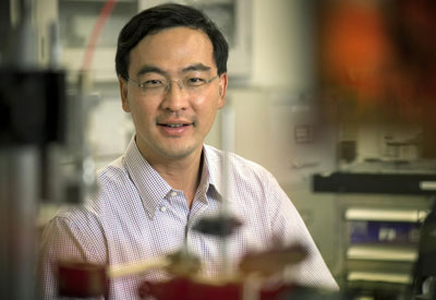 |
| This is Weidong Zhou, UTA electrical engineering professor.
|
|
"Big companies like IBM and Intel are using this technology for high-performance computing centers," Zhou said. "The big push now is for the next big thing: smaller, faster, and less and less power consumption."
|
|
Zhou also has recently received a three-year, $935,000 grant from the Air Force Office of Scientific Research to explore extreme energy efficiency lasers, in collaboration with Professors Shanhui Fan at Stanford and Xiuling Li at the University of Illinois Urbana-Champaign.
|
|
The projects point to an increasingly important role The University of Texas at Arlington is playing in the world of lasers and how they work on semiconductors.
|
|
Zhou is a Fellow of the International Society for Optical Engineering. He holds three issued patents related to this technology and has more than 270 journal publications and conference presentations. He joined UTA in 2004 after a brief career in industry.
|
|
A paper, entitled, "Printed Large-Area Single-Mode Photonic Crystal Bandedge Surface-Emitting Lasers on Silicon", was published online last month in Nature's Scientific Reports. It outlined Zhou's findings from related research supported by the National Science Foundation, the Air Force Office of Scientific Research and the Army Research Office.
|
|
His previous research led to innovations that removed roadblocks to putting optical technology on a silicon chip.
|
|
Specifically, Zhou developed a membrane laser less than one micron thick that is compatible with planar Complementary Metal Oxide Silicon platforms, which are the building blocks for all electronics and can be easily integrated with current platforms. The key innovation is the integration of certain compound semiconductor material with a silicon photonic crystal cavity, which allows a laser to be built directly on a silicon chip next to other electrical components. This leads to higher speed and higher efficiency.
|
|
The first application of Zhou's laser is in computers and data centers where higher bandwidth and transfer rates at lower energy outputs are prized. Zhou's group is actively pursuing various innovative membrane laser architectures for extreme energy efficient computing and communication systems. Zhou and collaborators will use his new grant to continue innovations in high-performance membrane lasers, including the one reported in Nature Photonics in 2012, entitled, "Transfer printing stacked nanomembrane lasers on silicon."
|
|
"We are looking for devices and components to be integrated on a chip," Zhou said. "As we address electrical injection, integration with other devices on the chip and increased power capabilities, we can begin to apply this technology to products in the medical field or in the consumer arena. These applications could include portable electronics, sensing and imaging equipment, bio applications and wearable electronics."
|

