| Posted: Feb 17, 2016 |
Match-head nanowire structures boost photovoltaic efficiency(Nanowerk News) Crystal growth on a nano/microscale level results in the formation of “match-head”-like, three-dimensional structures that enhance light absorption and photovoltaic efficiency (ACS Nano, "Si Radial p-i-n Junction Photovoltaic Arrays with Built-In Light Concentrators"). |
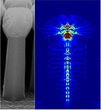 |
| The match-head structure acts as a built-in light concentrator and enhances optical absorptance and external quantum efficiencies by 30 to 40%, and PV efficiency under AM 1.5G illumination by 20% compared to cylindrical structures without match-heads. (© ACS) |
| Match-head semiconductor nanowires focus incident light for greater overall efficiency. The match heads are naturally formed during the wire-growth process, which can be applied to various materials and structures for photonic and optoelectronic devices. This is the first large structure grown on a nanowire tip and it creates a completely new architecture for harnessing energy. |
| Enhanced light absorption and efficient, photogenerated carrier collection are essential characteristics of highly efficient solar cells. Nanowires with embedded radial junctions are promising building blocks for highly efficient photovoltaics because of their ability to achieve these two characteristics. |
| The new technology in this highlight provides a novel method for enhancing optical absorption and photovoltaic efficiency with crystal growth. Controlled silicon crystal growth on the tops of silicon wires creates a match-head structure. The match head acts as a light concentrator. |
| Light absorptance was increased by 36% and photovoltaic efficiency was increased by 20%. Because the match-head crystal is naturally grown and minimizes surface energy, this technique is applicable for a wide range of materials and device architectures to boost performance. |
| The ability to control the shape of the nanostructure is essential for manufacturing next-generation semiconductor devices, such as photodetectors and light emitters. |
| Source: U.S. Department of Energy, Office of Science |

