| Posted: Mar 21, 2016 |
New way to control particle motions on 2-D materials
(Nanowerk News) Researchers at MIT and other institutions have found a new phenomenon in the behavior of a kind of quasiparticles called plasmons as they move along tiny ribbons of two-dimensional materials such as graphene and TMDs (transition metal dichalcogenides), which have a hexagonal structure resembling chicken wire. The team found that these plasmons can be separated into two different streams moving in opposite directions at the edges of the ribbons, like traffic on a two-lane highway, without the need for strong magnetic fields or other exotic conditions.
|
|
The new research was carried out by MIT associate professor of mechanical engineering Nicholas X. Fang, recent PhD graduate from that department Anshuman Kumar, and four other researchers from the University of Wisconsin at Milwaukee, Hong Kong Polytechnic University, and the University of Minnesota. The work was reported in a paper in the journal Physical Review B ("Chiral plasmon in gapped Dirac systems").
|
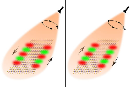 |
| Researchers used the spin of light to guide the flow of optical information. Shining right-circularly polarized light on nanoribbons made of special 2-D materials enables light to flow forward on one edge and backward on the other edge. Changing the polarization of the light causes the guided modes to reverse directions. (Image: Anshuman Kumar Srivastava)
|
|
Other groups had previously observed such separated flows, Fang says, but that previous work required the use of powerful magnetic fields. Instead, the new process relies largely on optical effects, he says, using beams of circularly polarized light.
|
|
The findings are based on exotic states of matter that can occur in two-dimensional materials that, unlike graphene, have a characteristic known as a bandgap, necessary for devices such as transistors or solar cells (and also in graphene that is modified to have a bandgap). These states of matter are based on quantum physics phenomena such as Berry curvature, which occur in configurations known as massive Dirac systems. Although such systems are a hot area of research these days, the researchers say this particular class of phenomena, involving surface electromagnetic properties known as surface plasmons, has been relatively unexplored until now.
|
|
Clustering in “valleys”
|
|
In the new work, the team showed that shining beams of circularly polarized light onto the graphene ribbons causes electrons in the material to cluster into two different “valleys” in the electronic band structure. The peculiar symmetry properties of this system gives rise to a phenomenon called Berry curvature, which can be thought of as an artificial magnetic field.
|
|
Under these conditions, these valleys correspond to motions of the plasmons — which are a kind of oscillation of electron density in the material — in opposite directions on the two edges of the material. The graphene ribbons are just 50 nanometers in width.
|
|
This effective magnetic field can be measured by sending in a second polarized beam, whose transmission can then be detected so that the changes in its polarization give a direct measurement of the effects taking place in the surface plasmons.
|
|
“This is exciting,” Fang explains, because it opens up a whole new approach to both manipulating the electromagnetic behavior of such systems and measuring the results of these manipulations.
|
|
This could suggest possibilities for new kinds of electro-optical devices, he says. For example, some experimental photonic systems require devices called optical isolators, which prevent beams of light in precision optical systems from being reflected back to their source and causing interference. But these isolators, which require strong magnetic fields, are inherently bulky, he says, limiting the usefulness of such systems. “With this concept,” he says, “it’s possible to replace these bulky optical isolators with one monolayer of two-dimensional material.”
|
|
Chip-scale isolation
|
|
With such a system, Kumar says, it should be possible “to do chip-scale optical isolation without the need for a magnetic field.” To achieve the same degree of optical isolation that this system would provide with a beam of light, Kumar says, with a conventional system would require a magnetic field with a strength of 7 tesla — a very strong field that would require a special research facility. (By comparison, the Earth’s magnetic field measures just 32 millionths of a tesla).
|
|
Theoretically, this could lead to applications such as new types of memory devices where information could be both written and read by using beams of polarized light, making them relatively immune to electromagnetic or other kinds of interference, the researchers say.
|
|
“The concept presented in this paper is very interesting and exciting,” says Fengnian Xia, an assistant professor of engineering and science at Yale University, who was not involved in this work. He adds, “In the long run, it may be possible to construct an electrically tunable on-chip isolator based on this concept, which can be a very critical component in integrated optics.”
|

