| Posted: May 13, 2016 |
Spin-currents at metal-oxide interfaces for magnetic memories(Nanowerk News) Research reported in the Applied Physics Express describes the observation of spin-to-charge current conversion by spin pumping from a ferromagnetic permalloy to a Cu/BiO interface. The metal/insulator interface makes it easier to control the spin-charge current conversion with an external electric field. |
| This research is featured in the May 2016 issue of the online JSAP Bulletin ("Experimental observation of spin-to-charge current conversion at non-magnetic metal/Bi2O3"). |
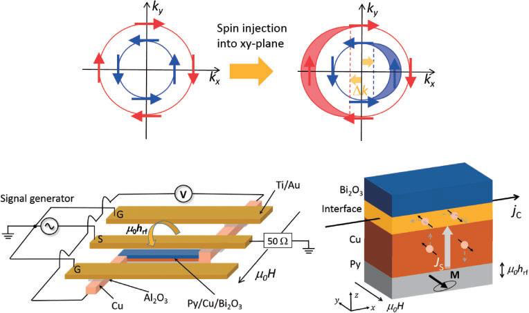 |
| Top: Fermi contours with Rashba splitting, and non-equilibrium spin accumulation resulting from a shift of Fermi contours by spin injection. Bottom left: Experimental setup for the spin pumping measurement. Bottom right: Schematic of spin-to-charge current conversion at the Cu/Bi2O3 interface. Spin currents are generated by spin pumping from a Py layer in ferromagnetic resonance to a Cu layer and reach a Cu/Bi2O3 interface. Then, the spin-to-charge current conversion occurs owing to the spin-momentum locking at the Rashba interface. (click on image to enlarge) |
| Devices based on spin currents rather than charge currents, offer interesting technological opportunities, such as future high-density, ultrafast and low-power magnetic memory devices. Conversion between charge and spin currents is key for exploiting such “spintronics”. Researchers at the University of Tokyo and RIKEN in Japan have now demonstrated spin-to-charge current conversion by spin pumping from a ferromagnetic permalloy (Py: Ni80Fe20) to a Cu/Bi2O3 interface. Importantly Cu/Bi2O3 is a metal/insulator interface, making it easier to control the spin-charge current conversion with an external electric field in the future. |
| One way of converting between charge and spin currents is by exploiting the interactions between electron’s spin and its motion, described as spin-orbit coupling (SOC). Heavy metals typically have large SOC but while spin-charge current conversion has been observed at Bi/Ag interfaces, applying an electric field at a metallic interface poses difficulties, hindering the possibility of controlling the conversion electrically. |
| Karube, Kondou and Otani fabricated trilayer 5 µm by 200 µm strips of 5 nm thick Ni80Fe20 (Py), 10 nm thick Cu, and 100 nm thick Bi2O3, and induced a ferromagnetic resonance in the Py using a Ti/Au waveguide alongside the multilayer. The voltage across the strip was then measured by sweeping the in-plane magnetic field applied perpendicular to the strip during application of 9 GHz rf current in the waveguide. |
| A clear peak corresponding to the spin-to-charge current conversion was observed in the voltage spectrum of the Py/Cu/Bi2O3 trilayer strip, but was absent when either Cu or Bi2O3 were omitted, highlighting the role of the Cu/Bi2O3 interface. The researchers conclude in their report, “We expect that this non-magnetic metal/Bi2O3 type interface will pave a way for controlling the conversion between spin and charge current by an electric field effect, which could be beneficial for domain wall motion and the magnetization switching.” |
| Source: Japan Society of Applied Physics |

