| Posted: Jun 07, 2016 |
New high-capability solid-state electron microscope detector enables novel studies of materials(Nanowerk News) At Cornell University, the Sol M. Gruner (SMG) detector group has developed and demonstrated a new type of imaging electron detector that records an image frame in 1/1000 of a second, and can detect from 1 to 1,000,000 electrons per pixel (Microscopy and Microanalysis, "High Dynamic Range Pixel Array Detector for Scanning Transmission Electron Microscopy"). This is 1000 times the intensity range, and 100 times the speed of conventional electron microscope image sensors. |
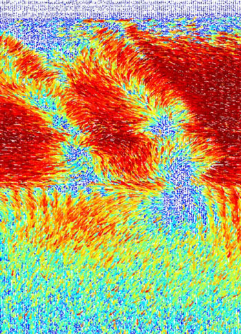 |
| This image might look like an impressionist sunset, but it is actually a vector map of the measured deflections of an atomic-sized electron beam scanned across different polar domains in the ferroelectric bismuth ferrite. The image was recorded in about a minute by the new electron microscope pixel array detector. |
| Capture of all the transmitted electrons allows quantitative measurement of materials properties, such as internal electric and magnetic fields, which are important for use of the materials in memory and electronics applications. |
| At Cornell University, we developed and tested a new detector for electron microscopes that enables quantitative measurements of electric and magnetic fields from micrometers down to atomic resolution. |
| The device is an adaptation of a solid-state x-ray detector technology we have developed over the last fifteen years, now modified to function as a high-speed, high dynamic range electron diffraction camera. Dynamic range denotes the maximum range of signals that can be detected by a pixel. |
| The resulting electron microscope pixel array detector records an image frame in under a millisecond, and can detect from 1 to 1,000,000 primary electrons per pixel per image frame. This is 1000 times the dynamic range, and 100 times the speed of conventional electron image sensors. |
| These properties allow us to record the entire unsaturated diffraction pattern in scanning mode, and simultaneously capture bright field, dark field, and phase contrast information, as well as analyze the full scattering distribution, opening the way for new multichannel imaging modes. From the analysis of the spatially resolved diffraction patterns, we can extract local strains, tilts, rotations, polarity, and even electric and magnetic fields. |
| Source: Department of Energy, Office of Science |

