| Posted: Jul 28, 2016 |
Getting light in shape with metamaterials(Nanowerk News) Converting light from one wavelength (or “color”) to a shorter wavelength, a process needed for efficient communication and advanced manufacturing, is typically inefficient. To tackle that inefficiency, a team built a specialized, layered structure with tiny metallic cavities that improves the light conversion efficiency by orders of magnitude. The cavities can also alter other characteristics (direction and polarization) of the outgoing light beam (Nature Communications, "Phased-array sources based on nonlinear metamaterial nanocavities" and Applied Physics Letters, "Enhanced optical nonlinearities in the near-infrared using III-nitride heterostructures coupled to metamaterials"). |
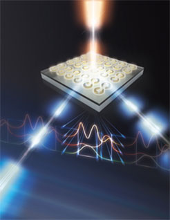 |
| Artist’s rendering of an incident laser beam (top of the figure) illuminating an array of nanoscale gold resonators on the surface of a “quantum well” semiconductor (slab in figure). (A quantum well is a thin layer that can restrict the movement of electrons to that layer.) The incoming laser beam interacts with the array and the quantum wells and is converted into two new laser beams with different wavelengths. Changing the size, shape, and arrangement of the resonators can be used for beam focusing, beam steering, or control of the beam’s angular momentum. (Image: Sandia National Laboratories) |
| The new concept explained in the studies can open doors for advanced lasers for optical communications and efficient manufacturing. It can also support efforts to miniaturize optical components for high-speed computing, telecommunications, cameras, and quantum computing that will solve computational problems currently intractable by today’s supercomputers. |
| This new concept involves arrays of optical nano-cavities called metamaterials, which are added to thin-layered semiconductors (heterostructures) to allow for efficient mediation of light. A “quantum well” (a designed semiconductor heterostructure that confines charge-carrying particles—such as electrons—to two-dimensional movement with distinct energy states) is used to convert one color of laser light to another. But it has been challenging to efficiently convert the laser light due to unfavorable quantum mechanical rules for these electronic transitions. |
| Now, researchers led by Sandia National Laboratories have made a system that effectively couples light into and out of the semiconductor quantum wells. The system creates intense light inside the quantum wells and can be designed to control the outgoing laser beam’s characteristics. |
| In this new structure, scientists designed nano-cavities following metamaterials concepts and fabricated the cavities on top of the semiconductor structure. The scientists designed the gold “C”-shaped nano-cavities to have special “resonance” frequencies that force the laser light to obey the rules imposed by the electronic transitions. When the resonance frequencies are made equal to the inter-subband transition energy, very efficient coupling of light into the quantum wells is achieved and light at twice the frequency (a process known as second-harmonic-generation) is generated inside the quantum well. Because the cavities were also designed to have a resonance at the new frequency, the nano-cavities efficiently radiate the light outwards. |
| Another interesting feature of the nano-cavities is that their arrangement on the surface allows one to determine the outgoing laser beam’s shape and polarization. This allows for new capabilities to control optical beams, creating new functionality. |
| The design of the nano-cavities and choice of the “quantum wells” allows for arbitrary shapes and energies of the resulting beam—across most of the infrared spectrum which can be useful for a wide range of applications. |
| Source: Sandia National Laboratories |

