| Posted: Aug 18, 2016 |
X-ray optics on a chip(Nanowerk News) Waveguides are widely used for filtering, confining, guiding, coupling or splitting beams of visible light. However, creating waveguides that could do the same for X-rays has posed tremendous challenges in fabrication, so they are still only in an early stage of development. |
| In the latest issue of Acta Crystallographica Section A: Foundations and Advances ("Miniaturized beamsplitters realized by X-ray waveguides"), Sarah Hoffmann-Urlaub and Tim Salditt report the fabrication and testing of a millimetre-sized chip capable of splitting a beam of X-rays. |
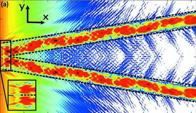 |
| Dashed lines mark the channel boundaries and the enlarged part displays the region where the wave is coupled in. The intensity is normalized and plotted in logarithmic scaling. (Image: Hoffmann-Urlaub and Salditt) |
| Fork-shaped channels that are only a few tens of nanometres wide and deep are transferred into a silicon wafer using electron-beam lithography and reactive ion etching then enclosed by bonding a second silicon wafer on top. |
| The results of simulations of how the 'parent' beam is split into two 'daughter' beams on passing through the chip were backed up by experimental measurements at the European Synchrotron Radiation Facility, showing that the incident beam is efficiently transported through the chip, neatly split and guided to exits that have precisely controlled (and tunable) spacings. After the daughter beams leave the chip, they interfere, leading to a pattern of vertical stripes just like the pattern obtained from a classical Young's double-slit interference experiment. |
| Interestingly, on close inspection there are fork-like structures within the stripes that originate from discontinuities in the phase of the recombined beam, forming striking features known as phase vortices. Furthermore, from those interference patterns the intensity distribution in the exit plane of the channels is reconstructed, which is found to be in very good agreement to the actual channel design. |
| This study complements earlier work on two-dimensionally confined channels in silicon in straight and tapered geometries, and paves the way to realizing `X-ray optics on a chip'. Illumination of samples by the two beams could provide some interesting advantages for coherent imaging and opens up the possibility of a new form of nano-interferometer. The authors envisage future development of their beamsplitter to create several daughter beams from the same parent beam, which would allow a single object to be imaged simultaneously by several beams, each from a different direction. |
| Source: International Union of Crystallography |

