| Posted: Nov 11, 2016 |
Low-resistance contacts move germanium electronics forward(Nanowerk News) Researchers at the University of Tokyo demonstrate that using germanides of metals at the metal-germanium interface with suitable surface crystal planes, greatly improves the contact resistance and device performance germanium semiconductor devices. The findings are reported in Applied Physics Express ("Reexamination of Fermi level pinning for controlling Schottky barrier height at metal/Ge interface"). |
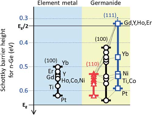 |
| Experimentally obtained Schottky barrier height (SBH) at element metal/n-Ge and germanide/n-Ge interfaces. By designing the metal and interface structure of Ge, the SBH at the direct metal/n-Ge interface is controllable to be less than half of the band gap of Ge. |
| The semiconducting element germanium is attracting great interest for next-generation electronics on account of its high electron and hole mobilities. However although high-mobility germanium transistor devices such as metal-insulator field-effect transistors (MISFETs) have been demonstrated, parasitic resistance and the suppression of off-state leakage at the source and drain gates still inhibit the performance of these devices. Now researchers at the University of Tokyo have demonstrated that using germanides of metals at the metal-germanium interface, and having the right crystal plane at the surface can greatly improve the contact resistance and device performance. |
| A difference in the energy levels of the band structure in a metal and a semiconductor can cause a barrier obstructing the transport of electrons - the “Schottky barrier height” (SBH). One of the main contributors to the contact resistance in germanium devices is “Fermi level pinning”, where band bending at the interface increases the SBH. |
| One hypothesis for the origin of Fermi level pinning is that a dipole is induced where the tail of the electron wavefunction meets the metal surface. This effect should be reduced when the electron density at this surface is decreased. The free electron density of metal germanides is typically 1-2 orders of magnitude less than metals, and when Tomonori Nishimura, Takeaki Yajima, and Akira Toriumi measured the current voltage characteristics at metal-germanides interfaces, they found the Fermi level pinning effects greatly alleviated. |
| The researchers also noted that the SBH was only diminished when the (111) crystalline plane was used. When the contact was made along the (110) plane the barrier to electron transport at germanium-germanide interfaces remained high. In their report of the findings they conclude, “these findings indicate that the SBH at the direct metal-Ge interface is practically controllable, and the contact resistance in Ge n-MISFETs can be considerably reduced.” |
| Source: Japan Society of Applied Physics |

