| Posted: Nov 30, 2016 |
Mix and match lasers(Nanowerk News) Combining silicon with a light-producing semiconductor may help develop micrometer-scale lasers, shows Doris Keh-Ting Ng and her colleagues from the A*STAR Data Storage Institute (Optics Letters, "Hetero-core III-V/Si microlaser"). |
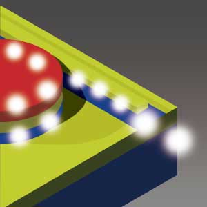 |
| A microlaser comprised of a cylinder of indium gallium arsenide phosphide (red) on silicon (blue) could enable integrated optical circuits. (Image: A*STAR Data Storage Institute) |
| Silicon has revolutionized the manufacture of electrical devices. This abundant semiconductor is easily processed into tiny components, such as transistors, using methods that are scalable to industrial levels, thus enabling the production of hundreds of thousands of elements on a single chip. Electronic engineers would like to further expand the functionality of these integrated circuits by enabling them to create, manipulate and detect light. |
| These optoelectronic devices could speed up processing of digital information, and lead to micrometer-scale lasers, for use in barcode scanners for example. The problem, however, is that silicon is not an efficient light generator. |
| Ng’s team designed and produced a laser compatible with silicon fabrication techniques by combining silicon and another semiconductor material that can produce light: indium gallium arsenide phosphide (InGaAsP). “Our results demonstrate a promising approach for efficient and compact active optoelectronic devices on silicon using a very thin III-V semiconductor layer,” says Ng. |
| A crucial consideration in any laser structure is optical feedback: the ability to trap light within the structure to drive further light generation. In conventional lasers, this is done by placing a mirror on either side of the light-generating region. Instead, Ng and the team used a cylindrical device geometry. This trapped some of the generated light at the walls of the device and forced it to propagate round inside the cylinder. This is called a whispering gallery mode because the same effect traps sound waves in a circular room such as a cathedral dome. |
| The team started with a silicon substrate, on to which they deposited a thin layer of silicon oxide. The optically active InGaAsP film, just 210 nanometers thick, was fabricated separately and then bonded on top of the silicon oxide. The team then etched through some of the material to create cylinders either two or three micrometers in diameter. The three-micrometer devices emitted laser light with a wavelength of 1,519 nanometers, very close to that used in commercial optical communications systems. |
| A unique feature of this device is that the whispering gallery mode extends over both the silicon and the InGaAsP regions. The InGaAsP provides light amplification while the silicon passively guides the light. “Next we hope to apply these ideas to devices operating at room-temperature,” says Ng. “Operation at higher temperature will require fine-tuning of the laser design and fabrication.” |
| Source: A*STAR |

