| Posted: Dec 05, 2016 |
How to 3D-print on the nanoscale(Nanowerk News) Realization of “3D printing” material assembly on the micron or even nanometer scale has posed significant challenges to researchers. Now, scientists have developed a specialized computer simulation that guides an electron beam to create custom 3D structures (ACS Nano, "Simulation guided 3D nanomanufacturing via focused electron beam induced deposition"). |
| The beam induces a precursor material to deposit in a way that forms complex shapes. This nanoscale 3D printing creates freestanding structures so tiny that bacteria dwarf them. |
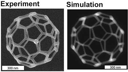 |
| A 32-face 3D truncated icosahedron mesh was created to test a simulation’s ability to guide precise construction of complex geometries. Scanning electron microscopy of the product (left) showed excellent agreement with the nanoscale structure that the simulation predicted (right). (© American Chemical Society) |
| The new approach, simulation-guided material deposition at the nanoscale, offers a path to synthesize materials with superior mechanical and optical properties. This design approach replaces trial-and-error in nanomanufacturing for materials and structures with superior mechanical and optical properties. |
| Precision control of nanometer scale 3D fabrication has been a longstanding research goal. Now, researchers have developed a 3D simulation that guides focused electron beam induced deposition (FEBiD) of precursor molecules on a surface and accurately predicts the complex geometries of deposited shapes over the length scale from nanometers to micrometers. |
| The simulation predicts gas-solid interactions where the electron beam strikes a surface. While FEBiD can direct-write freestanding 3D nanostructures, improved understanding of the dynamic interplay of the scanning electron beam and adsorbed precursor molecules is critical for advancing additive manufacturing of optoelectronics, metamaterials, and more. |
| The simulations consist of (1) a Monte Carlo simulation to calculate the electron–solid interaction and (2) a continuum simulation to calculate surface adsorption, desorption, diffusion, and deposition of precursor molecules. |
| The merged simulation can guide the electron beam to produce complex lattices and meshes sized between 10 nanometers and 1 micron. |
| Source: Oak Ridge National Laboratory |

