| Posted: Dec 06, 2016 |
Anomalously large charge transfer in an atomic layer cake of transition metal oxides
(Nanowerk News) Along with the critically important goal of making the next generations of electronics devices ever smaller, designers and developers also strive for multi-functionality. Traditional semiconductor-based microelectronic devices exploit interfacial charge transfer between different materials to create and manipulate electronic and magnetic states.
|
|
The spintronic approach to electronics, based not just on electric charge but on spin as well, requires further rethinking materials and structures. Designing technologically relevant materials and understanding how charge transfer occurs at their interfaces is a continuing challenge for heterojunctions based on strongly correlated electronic materials.
|
|
A team of researchers from the University of Arkansas, along with collaborators from the Indian Institute of Technology and Argonne National Laboratory, carried out studies at the U.S. Department of Energy’s Advanced Photon Source (APS) that demonstrate how massive charge transfer occurs in a synthesized heterostructure of transition metal oxides to create an unusual Mott insulating ground state at the atomic scale.
|
|
The work shows a path toward the development of electronics devices that are substantially more versatile and multifunctional than traditional semiconductors using various materials that could easily transition between a variety of electronic, magnetic, and spin states to achieve a wide range of functionalities in a single device.
|
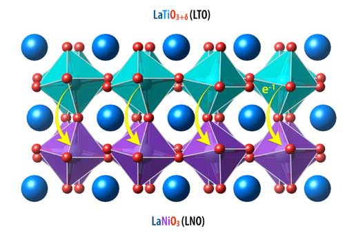 |
| Schematic of interfacial charge-transfer (yellow arrows) at the atomic scale in a heterostructure between doped Mott insulator LaTiO3+δ (top) and negative charge-transfer metal LaNiO3 (bottom).
|
|
Their study was published in Nature Communications ("Engineered Mott ground state in a LaTiO3+δ/LaNiO3 heterostructure").
|
|
Complex oxide interfaces have been found to offer tremendous possibilities for electronic and magnetic states that are unattainable with conventional semiconductors. Recent work has pointed toward a prominent role of partially filled d-shell transition metal ions in the phenomena connected to strongly correlated insulator behavior.
|
|
The current work builds upon those ideas to examine an interface between a charge-transfer metal, LaNiO3 (LNO) and a doped Mott-Hubbard insulator, LaTiO3+δ (LTO). The team synthesized atomically thin Mott–Hubbard insulator/charge-transfer metal heterostructures and investigated them with resonant soft x-ray spectroscopy at X-ray Science Division (XSD) beamline 4-ID-C and diffraction at XSD beamline 6-ID-B, both of the APS, an Office of Science user facility at Argonne.
|
|
The structure referred to as an LTO/LNO superlattice, was studied by x-ray absorption spectroscopy (XAS) and in situ x-ray photoemission spectroscopy (XPS) to determine how charge transfer operated in the novel interface. The experiment revealed an unexpected massive charge flow across the interface from titanium (Ti) to nickel (Ni) ions. Thus, the final state of Ni in the superlattice shows a state very close to Ni2+ within the chemical matrix originally supporting Ni3+.
|
|
The team next investigated how this modified interfacial band structure alters the physical properties. X-ray absorption spectroscopy revealed an unusual electronic configuration of Ni 3d8, d7, and d8L states at the interfacial NiO2 layer. A reconstruction of the band structure near the interface was also confirmed, with the splitting of the Ni eg band gap of about 0.20 eV. Another bandgap of about 1.3 eV is seen between the Ti 3d and Ni eg bands. Such a gap splitting has not been observed in other LNO-based heterojunctions.
|
|
The unusual insulating Mott ground state of the LTO/LNO heterostructure is an example of how the manipulation of charge transfer can create exotic states not only in the electronic domain but also with orbital and spin degrees of freedom.
|
|
The researchers expect that further research involving other types of charge-transfer interfaces will open up even more intriguing possibilities for the eventual realization of electronics components with capabilities far beyond those in current semiconductors.
|

