| Posted: Dec 07, 2016 |
Record tunneling magnetoresistance for very small perpendicular magnetic tunnel junctions(Nanowerk News) International Electron Devices Meeting 2016 (IEDM) —Dec. 6, 2016— At the 2016 IEEE International Electron Devices Meeting, in a special poster session on MRAM, world-leading research and innovation hub for nano-electronics and digital technology imec presented a 8nm p-MTJ device with 100 percent tunnel magnetoresistance (TMR) and coercive field as high 1500 Oe. |
| This world’s smallest device enables the establishment of a manufacturing process for high-density spin-transfer-torque magnetic random access memory (STT-MRAM) arrays that meet the requirements of the 10nm and beyond logic node for embedded non-volatile memory applications. It also paves the way for high density stand-alone applications. |
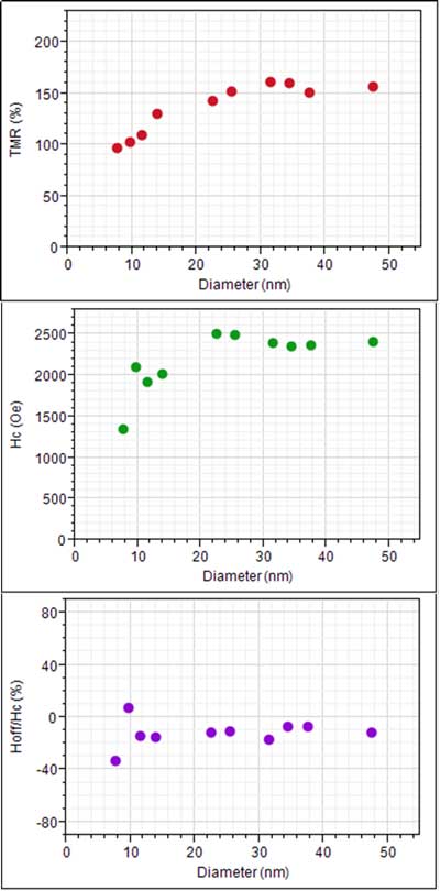 |
| (a) TMR (tunnel magnetoresistance), (b) Hc (coercivity) and (c) Hoff/Hc (offset field/coercivity, in %) across magnetic tunnel junctions of various sizes. (Image: imec) |
| STT-MRAM has the potential to become the first embedded non-volatile memory technology on advanced logic nodes for advanced applications and is also considered an alternative to conventional dynamic random access memory (DRAM). |
| The core element of an STT-MRAM is a magnetic tunnel junction (MTJ) in which a thin dielectric layer is sandwiched between a magnetic reference layer and a magnetic free layer, where writing of the memory cell is performed by switching the magnetization of the free layer. STT-MRAMs exhibit non-volatility, high-speed, low-voltage switching and nearly unlimited read/write endurance. |
| However, significant challenges towards commercialization remain, primarily in scaling the processes for higher densities and in increasing the device switching current. |
| In addressing these challenges, imec scientists have demonstrated for the first time an electrical functional p-MTJ device as small as 8nm. Despite the small dimensions, the device exhibits a high TMR of 100 percent, a coercivity (Hc) of 1500Oe and a spin torque efficiency -the ratio of the thermal stability and switching current- as high as three. The p-MTJ stack, featuring a free layer and reference layer of CoFeB-based multilayer stacks, was developed on 300mm silicon wafers and the fabrication process is compatible with the thermal budget of standard CMOS back-end-of-line (BEOL) technology. |
| Moreover, imec integrated arrays of p-MTJ devices into a 1T1MTJ structure to build STT-MRAM Megabit arrays with pitches down to 100nm, proving that the technology meets the dimensional requirements for the 10nm logic node and beyond. |
| “STT-MRAM is a promising memory concept for future technology nodes, but its scalability towards high densities has always been challenging,” stated Gouri Sankar Kar, distinguished member of technical staff coordinating RRAM, DRAM-MIMCAP, STT-MRAM activities at imec. “Our demonstration of a high-performance p-MTJ device as small as 8nm, combined with a manufacturable solution for a highly scalable STT-MRAM array will open up continued innovations for embedded non-volatile memory applications in the 10nm logic node.” |
| Source: imec |

