| Posted: Dec 13, 2016 |
Lightning-fast switch for electron waves
(Nanowerk News) The characteristic shine of metals is created by electrons which can freely move in the interior of the material and reflect incoming radiation. Similar to water waves on a pond, waves can form on the surface of this electron sea – so called “surface plasmons”. Instead of a stone that is thrown into water, light is used to generate surface plasmons in the laboratory. When light is focused onto a nanometer-sharp metallic tip, miniature waves propagate on the material’s surface in a circular fashion starting from the tip apex. A nanometer is only approximately ten times the size of the diameter of a single atom. The miniature waves could be used in future compact electronic devices for lightning-fast information transport.
|
|
So far, however, there has been no means of switching such surface waves on and off on ultrafast timescales, which is essential. Conversely, in conventional electronics the analogous mechanism is realized by transistors.
|
|
Now, for the first time, a team of scientists at the University of Regensburg, in collaboration with colleagues from Pisa, have demonstrated the experimental on/off switching of waves on the electron sea, laying the foundation for future plasma-electronics (Nature Nanotechnology, "Femtosecond photo-switching of interface polaritons in black phosphorus heterostructures").
|
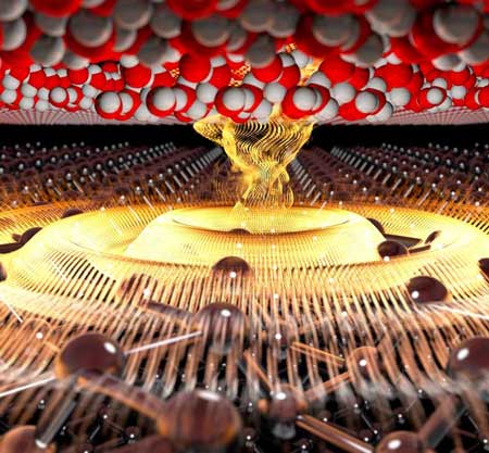 |
| In the heterostructure, waves of the plasma on black phosphorus (lower part) expand starting from the point of their excitation and cause the adjacent silicon dioxide (upper part) to oscillate. (Image: Fabian Mooshammer)
|
|
The key was that the physicists did not use a metal, where electron waves are always present. Instead a much more sophisticated heterostructure based on a semiconductor was developed by Miriam S. Vitiello and colleagues from Pisa for the study.
|
|
Semiconductors like, for example, silicon are the materials from which computer chips are made. The semiconductor in this heterostructure is an especially modern material: so-called “black phosphorus”. Upon irradiation by intense light pulses, freely moving electrons are generated inside the material. Without these electrons, no surface waves are present and the structure is switched “off”. However, as soon as the first laser pulse generates the free electrons, a subsequent pulse can start the propagation of surface plasmons from the tip.
|
|
To test how fast this switching process can take place, the team of Prof. Dr. Rupert Huber in Regensburg activated surface plasmons with ultrafast laser pulses that were as short as a few femtoseconds. One femtosecond is the unimaginably short time span of the millionth part of a billionth of a second, i.e. 0, 000 000 000 000 001 seconds.
|
|
Employing their worldwide unique microscope featuring nanometer spatial resolution in addition to ultrafast temporal resolution, the scientists subsequently traced the expansion of the plasmon waves in extreme slow motion snapshots. In this process it was clearly visible that the switching times where on the femtosecond scale, and thus many orders of magnitude faster than the fastest existing transistors.
|
|
As a pleasant surprise it was also found, that the wavelength of the surface waves is almost independent of the power of the laser which switches the structure.
|
|
These results are highly encouraging for future ultrafast electronics based on surface plasmons. In the next step, the scientists from Regensburg are testing first operational plasmonic components – on femtosecond time scales.
|

