| Posted: Dec 20, 2016 |
Revised Schottky diode equation for the graphene/semiconductor Schottky junction
(Nanowerk News) The Energy, Electron, Plasma and Plasmonic (EEPP) Group led by Prof. Ricky Ang at Singapore University of Technology and Design (SUTD) says that it has uncovered the underlying equation governing the carrier’s transport across the graphene/semiconductor Schottky junction, which is one of the building blocks in electronic and optoelectronic devices.
|
|
The paper was presented at the IEDM conference 2016 ("A modified Schottky model for graphene-semiconductor (3D/2D) contact: A combined theoretical and experimental study"; pdf).
|
 |
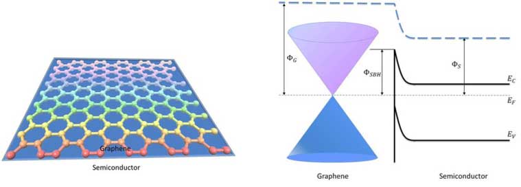
| Graphene/semiconductor Schottky junction. (click on image to enlarge)
|
|
Graphene, a single carbon atomically-thick layer, can be regarded as semimetal due to lack of band gap. It is considered promising metal candidate for next-generation devices, with its excellent transparency, mechanics, electronics and optical properties.
|
|
Traditionally, the Schottky diode equation is often used for characterization of I-V curve of metal/semiconductor contact. Thus researchers in the device community still blindly employ this “old” equation to interpret the “special” I-V characteristics of graphene/semiconductor Schottky contact, without questioning its validity.
|
|
However, the replacement of conventional metal with graphene radically changes the carrier’s transport process across graphene/semiconductor junction due to some changes in the interface properties.
|
|
Mr. Shi-Jun Liang, a PhD candidate supervised under Prof. Ricky Ang, proposed that “a new equation” should replace the old equation, which agrees well with much experimental data available. The SUTD research also predicts that this proposed equation is applicable to Schottky junction made of graphene and different dimensional semiconductor.
|
|
To fabricate excellent performance devices, researchers much first figure out how the Schottky barrier height (SBH) at the interface between graphene and semiconductor (3D/2D) is formed, which rectifies the carrier’s flow.
|
|
The STUD team discovered that formation mechanism for SBH is distinctive for different dimensional semiconductors. Due to the partial Fermi-level pinning (FLP) effect occurring at the junction of graphene and the 3D semiconductor (e.g. Silicon, SiC, GaAs, GaN, etc.), the SBH is weak dependence of doping of semiconductor.
|
|
In contrast, the SBH is nearly dependent of work function of 2D semiconductor (MoS2, MoSe2, WS2, WSe2, etc.).
|
|
Besides, they found that the inhomogeneous SBH formed at the interface of graphene and semiconductor contact is due to the electron-hole puddles induced by the impurities distributed on the surface of semiconductors, instead of ripples or defects created in the graphene.
|