| Posted: Dec 22, 2016 |
Spin filtering at room temperature with graphene
(Nanowerk News) An interdisciplinary team of scientists at the U.S. Naval Research Laboratory (NRL) have reported the first demonstration of metallic spin filtering at room temperature using ferromagnet-graphene-ferromagnet thin film junction devices (ACS Nano, "Room-Temperature Spin Filtering in Metallic Ferromagnet–Multilayer Graphene–Ferromagnet Junctions") – spin is a fundamental property of electrons, in addition to charge, that can be used to transmit, process and store data.
|
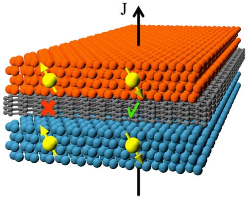 |
| Strain Measurement and Imaging Conceptual rendering of a spin-filtering graphene junction: Films of nickel (shown in blue) and iron (shown in red) contain a mixture of electrons with up and down spins. A few layers of graphene (shown in grey) lie between the metal layers to create a conductive path for electrons of one spin only, while blocking the other spin. A current driven though the metallic junction (labeled as 'J') becomes spin polarized. (Image: U.S. Naval Research Laboratory)
|
|
“The spin filtering had been theoretically predicted and previously seen only for high-resistance structures at cryogenic temperatures,” said Dr. Enrique Cobas, principal investigator, NRL Materials Science and Technology Division. “The new results confirm the effect works at room temperature with very low resistance in arrays of multiple devices.”
|
|
The thin film junctions demonstrated low resistance, and the magnetoresistance characteristic of a spin filter interface from cryogenic temperatures to room temperature. The research team also developed a device model to incorporate the predicted spin filtering by explicitly treating a metallic minority spin channel with spin current conversion, and determined that the spin polarization was at least 80 percent in the graphene layer.
|
|
“Graphene is famous for its extraordinary in-plane properties, but we wanted to look at conductivity between stacked graphene sheets and how they interact with other materials,” said Cobas.
|
|
To do so, NRL researchers developed a recipe to grow large multi-layer graphene films directly on a smooth, crystalline nickel alloy film while retaining that film’s magnetic properties, then patterned the film into arrays of cross-bar junctions.
|
|
“We also wanted to show we could produce these devices with standard industry tools, not just make one device,” Cobas added.
|
|
The spin filtering phenomenon is due to an interaction of the quantum mechanical properties of graphene with those of a crystalline nickel film. When the nickel and graphene structures align, only electrons with one spin can pass easily from one material to the other, an effect termed spin filtering, that results in spin polarization of an electric current.
|
|
“There is room for improvement as theory suggests the effect can be increased by an order of magnitude by fine-tuning the number of graphene layers,” said Dr. Olaf van ‘t Erve, research scientist, NRL Materials Science and Technology Division. “However, current models do not include the spin-conversion that happens inside the ferromagnetic contacts. Once we account for those effects, we’re already close to the ideal case of 100 percent spin polarization in the graphene layer, enabling us to revise our device geometry and materials to maximize the effect.”
|
|
The result is relevant to next-generation non-volatile magnetic random access memory (MRAM), which uses spin-polarized pulses to flip a magnetic bit from 0 to 1 and vice-versa. It may also find use in future spin logic technologies or as magnetic sensors.
|

