| Posted: Jan 29, 2017 |
Polycrystalline materials in solar cells gain new impulse(Nanowerk News) The conversion of sunlight into electricity through solar cells is considered to be a future cornerstone in a renewable energy supply for a sustainable society. The semiconducting compound Cu(In,Ga)Se2, which is deposited as a thin polycrystalline layer onto a metallized glass carrier, has long been known as an excellent light absorber. |
| In the last 5 years, the power conversion efficiency of solar cells based on this material has reached new record values, from ~19.8% in 2011 to 22.6% in 2016, within reach of those of the commercially dominating silicon wafer technology. These recent advances have been achieved through the introduction of a potassium-fluoride treatment of the Cu(In,Ga)Se2 material. |
| It is generally assumed that this treatment mainly affects the region of and near the charge-separating interface. |
| Researchers of the International Iberian Nanotechnology Laboratory (INL) in Braga have now demonstrated that also the electronic properties of the grain boundaries between the grains of the light absorbing layer are beneficially affected by the potassium treatment. |
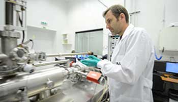 |
| Sascha Sadewasser in the Laboratory for Nanostructures Solar Cells © INL. |
| The study was performed in collaboration with researchers from the Institut des Matériaux Jean Rouxel (IMN) from the University of Nantes, who fabricated the solar cell samples and was published in Scientific Reports ("Effect of the KF post-deposition treatment on grain boundary properties in Cu(In, Ga)Se2 thin films"), an open access journal published by the Nature Group. |
| The researchers used an advanced scanning probe microscopy method to image electronic surface properties with nanometer-scale spatial resolution. |
| “We were able to show that the potassium treatment results in a stronger and more homogeneous electronic effect at the grain boundaries” says Nicoleta Nicoara, member of the Laboratory of Nanostructured Solar Cells at INL involved in the research. |
| Polycrystalline semiconductor materials can usually be fabricated more cost-efficient at lower processing temperatures compared to single-crystalline materials. However, the presence of grain boundaries limits their use in many applications, as they lead to losses in performance due to the presence of defects. |
| Sascha Sadewasser who led this study summarizes: “Our study demonstrates that the potassium fluoride treatment can beneficially modify the properties of grain boundaries in Cu(In,Ga)Se2 solar cell materials. The insight we gained through our study might well influence research directions in other polycrystalline materials, and animate researcher to search for treatments with similarly positive effects on the electronic properties of grain boundaries”. |
| Source: International Iberian Nanotechnology Laboratory |

