| Posted: Mar 07, 2017 |
Metallic atomically-thin layered silicon(Nanowerk News) A new metallic silicon (Si) nanostructure has been discovered by researchers from the London Centre for Nanotechnology, the Japan Advanced Institute of Science and Technology (JAIST), and the Brookhaven National Laboratory (BNL), USA. Their study, which appears in the journal 2D Materials ("Metallic atomically-thin layered silicon epitaxially grown on silicene/ZrB2"), shows that a new atomically-thin Si nanostructure with metallic properties can be grown upon the two-dimensional (2D) material silicene on zirconium diboride (ZrB2). |
| The new Si nanostructure is found to form an atomically-sharp edge with the 2D silicene sheet and could enable the development of native electrical contacting, an important step to realising functional devices based upon silicene and other 2D materials. |
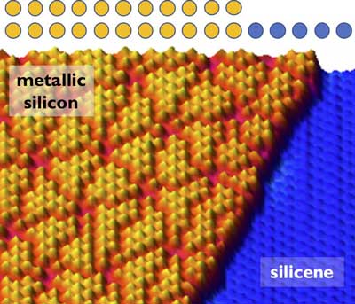 |
| Scanning tunnelling microscopy (STM) topographic image of the silicene surface on ZrB2 with (right) and without (right) an additional layer of silicon deposited on top. A schematic illustration of this is shown above. With the added layer, the silicon nanostructure becomes metallic and forms an atomically sharp boundary with the neighbouring silicene. |
| As the size of conventional semiconductor devices approaches the fundamental limit at the atomic scale, quantum mechanical effects begin to dominate their behaviour. Researchers across the globe are working to find new ways to harness these quantum phenomena, particularly in new materials in which their effects are more pronounced. One avenue of promise is research into materials that are only a few atomic layers thick. The first of these so called “atomically-thin 2D materials” to be realised in a laboratory was graphene, which is a single layer of carbon atoms. Since the discovery of graphene, a wide range of other 2D materials have been found that have a broad array of potentially novel properties. |
| “One very exciting new material is silicene, the silicon analogue to graphene” says Yukiko Yamada-Takamura, the member of the research team whose group first discovered the formation of silicene on ZrB2. “Silicene is an interesting development in the field because it may give us access to the electronic properties previously unique to graphene, but in the material of choice in the information technology industry, silicon.” |
| Recent work has shown that silicene can be incorporated into a conventional field effect transistor and other 2D materials. However, a challenge that remains is how to precisely electrically contact external wires to the silicene sheet without destroying the electronic properties that we desire. |
| In this work, the researchers found that growing additional silicon layers on top of the silicene surface led to the development of an unusual form of silicon that is unlike a normal silicon crystal. Using angle resolved photoelectron spectroscopy, a technique that probes how electrons are bound in a material, the team showed that the new Si nanostructure is metallic. Scanning tunnelling microscopy, an instrument capable of observing individual atoms on a surface, was then used to show that the transition to this metallic state occurs at atomically sharp boundaries, without affecting the properties of the neighbouring silicene sheet. |
| “This work highlights the unexpected and intriguing results that can manifest when the structure of 2D materials are altered, even by the addition of one more layer of atoms” said Dr Tobias G. Gill, the first author of this work. “We hope that this new metallic form of silicon can be used to develop the ability to produce native electrical contacts to silicene in future devices.” |
| Source: London Centre for Nanotechnology |

