| Posted: Mar 07, 2017 |
Hexagonal boron nitride enables the fabrication of 2-dimensional electronic memories(Nanowerk News) The use of two dimensional (2D) layered materials to improve the capabilities of electronic devices is a promising strategy that has recently gained much interest in both academia and industry. However, while the research in 2D metallic and semiconducting materials is well established, detailed knowledge and applications of 2D insulators are still scarce. |
| The research group lead by Dr. Mario Lanza, a Young 1000 Talent Professor born in Barcelona (Spain) and based in Soochow University (China), is leading a global effort to investigate the properties of layered dielectrics. |
| In his recent Advanced Functional Materials paper ("Coexistence of Grain-Boundaries-Assisted Bipolar and Threshold Resistive Switching in Multilayer Hexagonal Boron Nitride"), Prof. Lanza and co-workers engineered a family of resistive random access memories (RRAM) using multilayer hexagonal boron nitride (h-BN) as dielectric. |
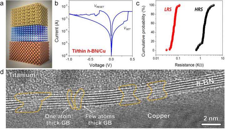 |
| (a) Schematic of a Ti/thin h-BN/Cu RRAM device. (b) Typical I-V curves in a Ti/thin h-BN/Cu RRAM device showing bipolar RS. (c) Cumulative distribution of the resistance per cycle in HRS and LRS read at 0.1 V. (d) Cross-sectional TEM image showing defective paths (GBs) through the h-BN. (© Wiley) (click on image to enlarge) |
| The patented devices show the coexistence of forming free bipolar and threshold-type resistive switching (RS) with low operation voltages down to 0.4 V, high current on/off ratios up to 1,000,000, and promising retention times above 10h, as well as low cycle-to-cycle and device-to-device variability. The RS is driven by the grain boundaries (GBs) in the polycrystalline h-BN stack, which allow the penetration of metallic ions from adjacent electrodes. This reaction can be boosted by the generation of B vacancies, which are more abundant at the GBs. |
| This investigation has been developed in collaboration with The Massachusetts Institute of Technology, Stanford University and Harvard University (among others). These results may have essential implications for the development of digital electronic devices made of 2D materials. |
| Source: Lanzalab |

