| Posted: Mar 24, 2017 |
Multi-parameter microscopy aids design of improved optoelectronic devices(Nanowerk News) The National Physical Laboratory (NPL) has developed a novel measurement method, providing simultaneous topographical, electrical, chemical and optical microscopy (STEOM) at the nanoscale for the first time (Nanoscale, "Simultaneous topographical, electrical and optical microscopy of optoelectronic devices at the nanoscale"). |
| The new method can be used to optimise the performance of optoelectronic devices such as organic solar cells, sensors and transistors. |
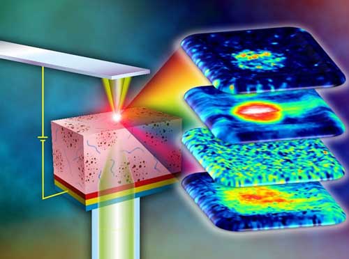 |
| The STEOM apparatus for multi-parameter characterisation of optoelectronic devices at the nanoscale. |
| As part of an international collaboration, NPL researchers demonstrated the direct application of the new method to the optimisation of organic solar cells. Transparent, flexible and low-cost organic solar cells could offer a solution to large-scale, low-carbon energy generation. |
| However, a lack of analytical techniques that can simultaneously probe device properties at the nanoscale has presented a major obstacle to their optimisation. |
| The new STEOM method developed at NPL addresses this problem, providing simultaneous measurements of topography and electrical, chemical and optical properties, while also being non-destructive, causing no damage to the samples being measured. |
| The breakthrough was achieved by combining plasmonic optical signal enhancement with electrical-mode scanning probe microscopy. This allows the relationship between surface morphology, chemical composition and current generation in operating organic solar cells to be explored at the nanoscale for the first time. |
| The team demonstrated that information gained using the method can successfully explain the performance of organic solar cells in terms of the nanoscale composition of their active surface layer, and could be used to identify the best routes for device optimisation. |
| In addition to organic solar cells, the method can be applied to a range of different problems where nanoscale electronic properties are influenced by surface composition and could consequently be used to guide the design of improved optoelectronic devices, from sensors to LEDs. |
| Source: National Physical Laboratory |

