| Posted: Apr 11, 2017 |
'Neuron-reading' nanowires could accelerate development of drugs for neurological diseases
(Nanowerk News) A team led by engineers at the University of California San Diego has developed nanowires that can record the electrical activity of neurons in fine detail. The new nanowire technology could one day serve as a platform to screen drugs for neurological diseases and could enable researchers to better understand how single cells communicate in large neuronal networks.
|
|
"We're developing tools that will allow us to dig deeper into the science of how the brain works," said Shadi Dayeh, an electrical engineering professor at the UC San Diego Jacobs School of Engineering and the team's lead investigator.
|
|
"We envision that this nanowire technology could be used on stem-cell-derived brain models to identify the most effective drugs for neurological diseases," said Anne Bang, director of cell biology at the Conrad Prebys Center for Chemical Genomics at the Sanford Burnham Medical Research Institute.
|
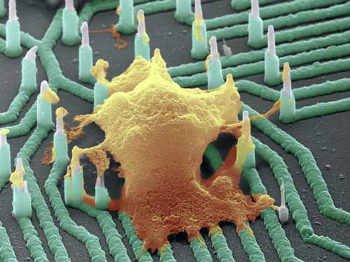 |
| This is a colorized SEM image of a neuron (orange) interfaced with the nanowire array. (Image: Integrated Electronics and Biointerfaces Laboratory, UC San Diego) (click on image to enlarge)
|
|
The project was a collaborative effort between the Dayeh and Bang labs, neurobiologists at UC San Diego, and researchers at Nanyang Technological University in Singapore and Sandia National Laboratories. The researchers published their work Apr. 10 in Nano Letters ("High Density Individually Addressable Nanowire Arrays Record Intracellular Activity from Primary Rodent and Human Stem Cell Derived Neurons").
|
|
Researchers can uncover details about a neuron's health, activity and response to drugs by measuring ion channel currents and changes in its intracellular potential, which is due to the difference in ion concentration between the inside and outside of the cell. The state-of-the-art measurement technique is sensitive to small potential changes and provides readings with high signal-to-noise ratios. However, this method is destructive -- it can break the cell membrane and eventually kill the cell. It is also limited to analyzing only one cell at a time, making it impractical for studying large networks of neurons, which are how they are naturally arranged in the body.
|
|
"Existing high sensitivity measurement techniques are not scalable to 2D and 3D tissue-like structures cultured in vitro," Dayeh said. "The development of a nanoscale technology that can measure rapid and minute potential changes in neuronal cellular networks could accelerate drug development for diseases of the central and peripheral nervous systems."
|
|
The nanowire technology developed in Dayeh's laboratory is nondestructive and can simultaneously measure potential changes in multiple neurons -- with the high sensitivity and resolution achieved by the current state of the art.
|
|
The device consists of an array of silicon nanowires densely packed on a small chip patterned with nickel electrode leads that are coated with silica. The nanowires poke inside cells without damaging them and are sensitive enough to measure small potential changes that are a fraction of or a few millivolts in magnitude. Researchers used the nanowires to record the electrical activity of neurons that were isolated from mice and derived from human induced pluripotent stem cells. These neurons survived and continued functioning for at least six weeks while interfaced with the nanowire array in vitro.
|
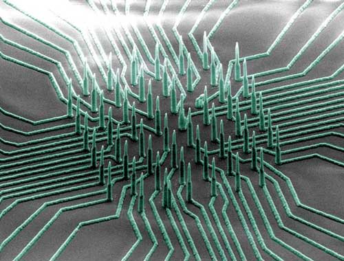 |
| This is a colorized SEM image of the nanowire array. (Image: Integrated Electronics and Biointerfaces Laboratory, UC San Diego)
|
|
Another innovative feature of this technology is it can isolate the electrical signal measured by each individual nanowire. "This is unusual in existing nanowire technologies, where several wires are electrically shorted together and you cannot differentiate the signal from every single wire," Dayeh said.
|
|
To overcome this hurdle, researchers invented a new wafer bonding approach to fuse the silicon nanowires to the nickel electrodes. Their approach involved a process called silicidation, which is a reaction that binds two solids (silicon and another metal) together without melting either material. This process prevents the nickel electrodes from liquidizing, spreading out and shorting adjacent electrode leads.
|
|
Silicidation is usually used to make contacts to transistors, but this is the first time it is being used to do patterned wafer bonding, Dayeh said. "And since this process is used in semiconductor device fabrication, we can integrate versions of these nanowires with CMOS electronics." Dayeh's laboratory holds several pending patent applications for this technology.
|
|
Dayeh noted that the technology needs further optimization for brain-on-chip drug screening. His team is working to extend the application of the technology to heart-on-chip drug screening for cardiac diseases and in vivo brain mapping, which is still several years away due to significant technological and biological challenges that the researchers need to overcome. "Our ultimate goal is to translate this technology to a device that can be implanted in the brain."
|


