| Posted: Apr 20, 2017 |
Smallest transistor ever
(Nanowerk News) It has long been thought that building nanometer-sized transistors was impossible. Simply put, the physics and atomic structural imperfections couldn’t be overcome. However, scientists built fully functional, nanometer-sized transistors. They did so using atomically flat, two-dimensional molybdenum disulfide semiconductor and a single-walled carbon nanotube imbedded in zirconium dioxide (Science, "MoS2 transistors with 1-nanometer gate lengths").
|
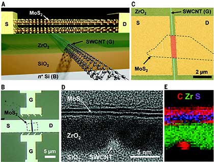 |
| Schematic of the smallest field effect transistor ever made shows the components of the transistor. The current flowing through the atomically thin molybdenum disulfide (MoS2) material, placed between the source (S) and drain (D) terminals, is controlled by the voltage applied to the 1-nanometer-thick single-walled carbon nanotube (SWCNT), imbedded in zirconium dioxide (ZrO2) dielectric material. The atomic structure of the layers in the transmission electron microscope image on the right shows the nanotube embedded in the ZrO2 layer and resting on a silicon dioxide (SiO2) layer. The width of the nanotube is less than 1/1000th of the diameter of a red blood cell.
|
|
Moore’s law states that the number of transistors per square inch on a microchip has doubled every year since they were invented. This has been realized by the ability to decrease the size of a transistor. However, when the gate length of the transistors approaches 5 nanometers, it was believed that our ability to continue to shrink a transistor size would reach its limit.
|
|
Below this feature size, it was not clear how to build next-generation devices. The result of this research shows that it is feasible to continue to reduce the size of a transistor, all the way down to 1 nanometer.
|
|
The next generation of microelectronics will only be realized by finding ways to continue to reduce the size of a transistor. Since the introduction of integrated circuits, the observation referred to as Moore’s law has been met — about every year, the number of transistors per unit area has doubled continuously, which is a direct consequence of our ability to continue to decrease the size of a transistor.
|
|
The gate length of a transistor is the defining parameter of the transistor size, and is presently about 20 nanometers in commercial electronic chips.
|
|
It is not possible to shrink it below 5 nanometers using silicon. However, researchers have demonstrated that using the semiconducting material molybdenum disulfide (MoS2) and single-walled carbon nanotubes, the transistor gate length can be reduced to a record size of 1 nanometer.
|
|
The team used these materials to fabricate a fully operational transistor. These novel materials are atomically uniform at a thickness down to a monolayer.
|
|
In comparison to current materials, these newly discovered materials have lower dielectric constants, larger band gaps, and a larger carrier effective mass making them ideally matched to the device requirements.
|
|
The characteristics of the nanometer-sized transistor have been measured and show a subthreshold swing ~65 mV/decade and On/Off current ratio ~106.
|
|
This work demonstrated the shortest transistor ever and that Moore’s law can continue a while longer by proper engineering of the semiconductor material and device architecture.
|

