| Posted: May 30, 2017 |
A low-tech, solution-based route to high-performance carbon nanotube thin films
(Nanowerk News) Think of a computer chip that bends, rather than breaks. That’s the potential of a new study by scientists at Rice University and Los Alamos National Laboratory (Nature Nanotechnology, "Wafer-scale monodomain films of spontaneously aligned single-walled carbon nanotubes").
|
|
Making such a chip requires a rapid, simple route to self-organizing tiny carbon nanotubes into thin films.
|
|
The team’s method produces a film with millions of carbon nanotubes aligned and tightly packed, like water pipes on a flatbed truck.
|
|
The tubes are orders of magnitude better aligned than previously possible.
|
|
The team’s method for creating the film balances forces between the tubes and polymer membrane surfaces to harness a spontaneous self-alignment mechanism.
|
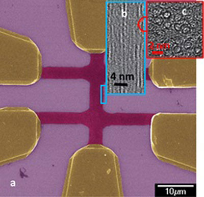 |
| A) Metal contacts (gold regions) connect to highly aligned carbon nanotube patterned films (red strips) to allow voltage control of their electrical properties. B) A close-up image of the films shows the high degree of carbon nanotube alignment. C) The cross section of the film shows the nanotubes are densely packed having about 1 million tubes per square micron (~1/10,000th the cross-sectional area of a human hair).
|
|
Assembly is a key challenge to fabricating flexible computer chips, displays, and other devices from carbon nanotubes. Self-assembly of the carbon nanotubes is particularly vital as one looks to integrate multiple devices into useful systems.
|
|
The researchers were up to the challenge. They harnessed a spontaneous self-alignment mechanism to create a fast way to produce the needed films. The films have applications in imaging, sensing and security.
|
|
Inside an individual carbon nanotube, electrons, phonons and excitons can travel in only one dimension. This property enables the tube to have electronic, optical and thermal properties that depend on direction.
|
|
For example, electrical current can flow along the length of the tube but not perpendicular to it. Tightly bundling millions of tubes together would greatly increase the current-carrying capacity. Despite significant efforts to produce large-scale architectures of aligned nanotubes, results have been limited.
|
|
In this study, scientists showed that films greater than a centimeter squared of aligned single-walled carbon nanotubes are possible by combining surfactant chemistry and slow vacuum filtration.
|
|
The nanotubes in the resulting films are aligned and tightly packed, with 1 million nanotubes in a cross-sectional area of one square micron (about 1/10,000 the cross-sectional area of a human hair). The method works for nanotubes created using various methods.
|
|
In addition, the method works with different lengths of nanotubes, meaning film thickness is controllable from a few nanometers to around 100 nanometers. Combining this method with recently developed carbon nanotube sorting techniques allows for highly aligned and chirality-enriched nanotube thin-film devices.
|
|
The team demonstrated how the films could be used as efficient terahertz polarizers and thin film transistors for optoelectronic applications.
|

