| Posted: Jun 28, 2017 |
Nanofabrication: A slick route to smart surfaces
(Nanowerk News) The phenomenon of ‘dewetting’ — usually considered a nuisance as it causes solids to bead up into islands, much like raindrops on glass — has been harnessed for a useful application.
|
|
An A*STAR-led team has clarified how dewetting can assemble arrays of 3D nanostructures for applications including single molecule sensing (Scientific Reports, "Nanostructure Formation by controlled dewetting on patterned substrates: A combined theoretical, modeling and experimental study").
|
|
Solid state films freshly applied to microelectronic devices sometimes split apart at temperatures much lower than typical melting points, due to the high energy at the interface between the film and substrate. This dewetting effect is increasingly problematic at nanoscale film dimensions; however it has also inspired researchers looking for an easy way to produce patterned substrates.
|
|
Liangxing Lu from the A*STAR Institute of High Performance Computing and co-workers recently demonstrated that metal films can be transformed into ‘nano-aperture’ arrays — tiny pores with dimensions controllable down to 10 nanometers — by performing dewetting on surface templates containing 3D ridges and ripples. However, the team found that the templates only produced nano-apertures from metal films of a certain thickness; otherwise, random nanodot features appeared.
|
 |
| Researchers have developed a recipe book of different nanopatterned surfaces possible by combining dewetting techniques with 3D surface templates. (Licensed under CC BY 4.0 © 2016 L. X. Lu et al.)
|
|
“Many factors influence the dewetting process, and also there are many types of equilibrium structures,” says Lu. “Finding the conditions for select morphologies is complex and difficult.”
|
|
To use dewetting for other nanostructure shapes, Lu and colleagues developed a custom algorithm to simulate solid state dewetting. Their technique calculates all possible nanopatterns for a dewetting film on a template and spots the lowest energy configuration. Then, diffusion calculations expose how movements between adjacent nano-islands lower the system’s total free energy.
|
|
“This model ignores the detailed kinetics, and instead analyzes the diffusion paths of equilibrium morphologies on a given substrate,” explains Lu. “The only driving forces are the surface and interface energies, which simplifies the problem.”
|
|
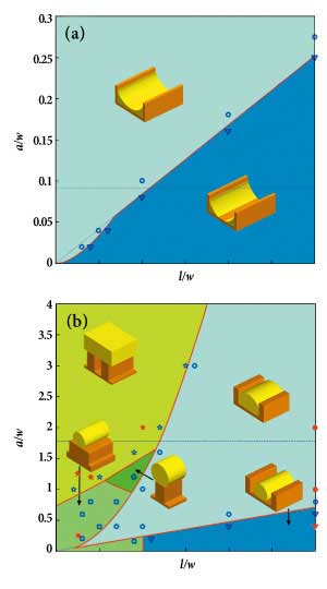
Through their calculations, the researchers produced detailed descriptions of droplet coalescence inside pit-shaped templates, and beading on top of table-like 'mesa' templates. Then, they generated phase diagrams that identified possible dewetting behavior on differently shaped templates — guidelines that proved useful for fabrication trials.
|
|
Collaborators at A*STAR’s Institute of Materials and Research Engineering verified this analytical approach by coating 100-nanometer high mesa templates with gold films, and then induced dewetting by heating the substrate. With electron microscopy images, they captured gold nanopatterns that matched their phase simulations, with only one exception: defects, such as grain boundaries, disrupted the natural dewetting patterns.
|
|
Lu believes that such fundamental fabrication insights could help optimize dewetting techniques for metallic interconnects and gratings, as well as the growth of special morphologies, such as nanowires.
|

