| Posted: Jul 08, 2017 |
Powerful new photodetector can enable optoelectronics advances
(Nanowerk News) In today’s increasingly powerful electronics, tiny materials are a must as manufacturers seek to increase performance without adding bulk.
|
|
Smaller also is better for optoelectronic devices — like camera sensors or solar cells — which collect light and convert it to electrical energy. Think, for example, about reducing the size and weight of a series of solar panels, producing a higher-quality photo in low lighting conditions, or even transmitting data more quickly.
|
|
However, two major challenges have stood in the way: First, shrinking the size of conventionally used “amorphous” thin-film materials also reduces their quality. And second, when ultrathin materials become too thin, they become almost transparent and actually lose some ability to gather or absorb light.
|
|
Now, in a nanoscale photodetector that combines a unique fabrication method and light-trapping structures, a team of engineers from the University of Wisconsin–Madison and the University at Buffalo has overcome both of those obstacles.
|
 |
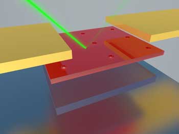
| Tuned to absorb specific light wavelengths, the new photodetector consists of nanocavities sandwiched between a ultrathin single-crystal germanium top layer and reflective silver on the bottom. (Image: Zhenyang Xia/UW-Madison College of Engineering)
|
|
The researchers — electrical engineering professors Zhenqiang (Jack) Ma and Zongfu Yu at UW–Madison and Qiaoqiang Gan at UB — described their device, a single-crystalline germanium nano-membrane photodetector on a nano-cavity substrate in the journal Science Advances ("Single-crystalline germanium nanomembrane photodetectors on a foreign substrate").
|
|
“The idea, basically, is you want to use a very thin material to realize the same function of devices in which you need to use a very thick material,” says Ma.
|
|
The device consists of nano-cavities sandwiched between a top layer of ultrathin single-crystal germanium and a reflecting layer of silver.
|
|
“Because of the nano-cavities, the photons are ‘recycled’ so light absorption is substantially increased — even in very thin layers of material,” says Ma.
|
|
Nano-cavities are made up of an orderly series of tiny, interconnected molecules that essentially reflect, or circulate, light. Gan already has shown that his nano-cavity structures increase the amount of light that thin semiconducting materials like germanium can absorb.
|
|
However, most germanium thin films begin as germanium in its amorphous form — meaning the material’s atomic arrangement lacks the regular, repeating order of a crystal. That also means its quality isn’t sufficient for increasingly smaller optoelectronics applications.
|
|
That’s where Ma’s expertise comes into play. A world expert in semiconductor nano-membrane devices, Ma used a revolutionary membrane-transfer technology that allows him to easily integrate single crystalline semiconducting materials onto a substrate.
|
|
The result is a very thin, yet very effective, light-absorbing photodetector — a building block for the future of optoelectronics.
|
 |
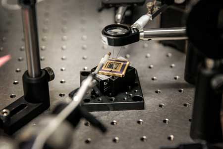
| Shrinking photodetectors like this scant wafer held in a frame for testing in the laboratory of UW–Madison engineering Professor Zhenqiang (Jack) Ma help make consumer electronics smaller. (Image: UW-Madison College of Engineering)
|
|
“It is an enabling technology that allows you to look at a wide variety of optoelectronics that can go to even smaller footprints, smaller sizes,” says Yu, who conducted computational analysis of the detectors.
|
|
While the researchers demonstrated their advance using a germanium semiconductor, they also can apply their method to other semiconductors.
|
|
“And importantly, by tuning the nano-cavity, we can control what wavelength we actually absorb,” says Gan. “This will open the way to develop lots of different optoelectronic devices.”
|


