| Posted: Jul 25, 2017 |
When shallow defects align, diamonds shine for unprecedented quantum sensitivity
(Nanowerk News) Imagine a sensor so sensitive it can detect changes in the proton concentration of a single protein, within a single cell. This level of insight would reveal elusive quantum-scale dynamics of that protein’s function, potentially even in real time, but demands a sensor with controllable features at a similar scale.
|
|
Thanks to a new fabrication technique, quantum sensing abilities are now approaching this scale of precision. As they report this week in Applied Physics Letters ("Perfectly aligned shallow ensemble nitrogen-vacancy centers in (111) diamond"), researchers in Japan have reproducibly formed an aligned ensemble of quantum sensors called nitrogen vacancy (NV) centers, just nanometers from its substrate’s surface.
|
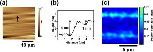 |
| Surface morphology and fluorescence characteristics of shallow ensemble NV centers. (a) AFM image (field view of 30 µm × 30 µm): black arrow indicates the <112> direction and the location of the cross sectional scan shown in (b). (b) AFM cross sectional profile. (c) XY confocal scan image (field of view of 10 µm x 10 µm). (© AIP)
|
|
Verified by nanoscale nuclear magnetic resonance (NMR) measurements, these results mark a clear path towards atomic level design of quantum sensors with larger surface areas than typically achievable. This is the first demonstration of this nanoscale NMR measurement with perfectly aligned, high-density NV centers near the surface, marking a huge advance for quantum magnetometry research.
|
|
“The way to combine both high counts and high contrast is to have the alignment, because when you have the alignment you basically have the benefit of the single NVs combined with the high counts obtained from the ensemble NV centers,” said Hitoshi Ishiwata from the Tokyo Institute of Technology and lead author of the paper. “So that’s what we basically did, really close to the surface -- within 10 nanometers -- and we demonstrated that with a SIMS [Secondary Ion Mass Spectrometry] measurement, as well as measuring nano NMR, which shows you the approximation of the distance of NVs from the surface.”
|
|
NV centers, already a popular tool in the world of quantum sensing, are specific kinds of impurities in the crystal structure of diamond. For a single unit of diamond’s otherwise purely carbon configuration, the NV center consists of a nitrogen atom adjacent to a missing (vacant) atom in the crystal’s lattice. This defect can occur in one of four possible locations in the unit crystal, and each provides a single-photon signal whose spectral signature is nuclear spin-dependent.
|
|
The new technique uses a combination of chemical vapor deposition (CVD) and directional polishing to control how the NVs form in the lattice. For their diamond substrate, which has a commonly aligned surface, where the lattice is oriented along the same crystollagraphic plane (called 111 in this case), Ishiwata and his colleagues achieved ensembles of NVs all with the same orientation. For a substrate measuring about 10 microns across, just less than the width of a human hair, their method can produce somewhere around 10,000 such centers within 10 nanometers from surface.
|
|
NVs in the same respective locations of their crystal units and so close to the surface, the group could conduct nanoscale NMR detection of the fluorine in oil making contact with the substrate. The reliability of their fabrication method has (literally) far reaching applications for wide field measurements, ensuring the high contrast detection over relatively large sample areas.
|
|
“The other benefit of high density NV centers with alignment is to perform wide field imaging with high sensitivity,” Ishiwata said. “Before it was impossible to have high sensitivity for wide field imaging due to the difficulty of obtaining alignment of NV centers with high density. With our technique, high contrast wide field imaging with high signal to noise ratio is now possible, which leads to high sensitivity wide field imaging.”
|
|
As the group continues to look for ways to further improve the method, they are also looking to explore applications of these ensembles in time resolved sensing, using pulsed lasers to provide real-time proton information of dynamic samples. Ishiwata himself was particularly excited about the possibilities for understanding biological cells like never before.
|
|
“A future application of this material is the observation of individual cell membranes because our material is suited for observing nanoscale NMR on the volume scale of 17 cubic nanometers, which is comparable to the thickness of cell membranes (~5 nanometers),” Ishiwata said. “So we could use this material and measurement technique for locally probing nanoscale activity of proteins that exists in cell membrane with high sensitivity.”
|

