| Posted: Jul 26, 2017 |
On-chip optics find their groove
(Nanowerk News) High-speed optical circuits and sensors generally require strict control over light polarization to minimize loss and cross-talk in photonic devices such as waveguides. An A*STAR team now predicts that noise resulting from imperfect polarizations can be eliminated using microstructures known as ‘slot’ waveguides (Scientific Reports, "Polarisation independent silicon-on-insulator waveguides").
|
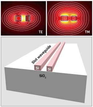 |
| Optimizing the layout of slot waveguides can eliminate differences in transverse electronic (TE) and magnetic (TM) light refraction, creating a single beam that is significantly easier to incorporate into photonic circuits. (Image: A*STAR Institute of High Performance Computing)
|
|
Discovered just over a decade ago, slot waveguides trap electromagnetic fields into a narrow region between two microfabricated strips of materials, such as silicon. Differences in the refractive indices between the slots and rails help focus the light into the slot with optical intensity and power not seen in typical waveguides. These properties impart improved sensitivity to sensors and generate useful amplification effects.
|
|
One difficulty with photonic waveguides, however, is splitting incoming radiation into electric and magnetic polarization components within nanometer-scale spaces.
|
|
“Inevitably, there will be contamination from the light source or defects along the waveguides,” says Jun Rong Ong from A*STAR’s Institute of High Performance Computing. “Unwanted polarization acts as noise, and this deteriorates device performance.”
|
|
Ong, along with colleagues Valerian Chen and Ching Eng Png, hypothesized that a special state known as ‘zero birefringence’ might negate the need for specialized splitter devices currently used in photonic waveguides. Birefringence describes how light with a mix of polarizations can refract into two directions when passing through crystals with specific shapes.
|
|
The team undertook a systematic theoretical analysis to determine if changes to the waveguide’s height, angle, and slot size could remove birefringence from the waveguide, leaving just a single ray.
|
|
“By having zero birefringence, we can process the inevitable mix of both polarizations simultaneously,” explains Ong. “This means the device footprint could be effectively halved.”
|
|
The trio’s simulations showed that many structural parameters could produce zero birefringence in the waveguide, but some were more effective than others. Surprisingly, they discovered the two rails need not be symmetric — having unequal widths enabled one side to confine greater amount of light, and give better control over the waveguide’s refractive index. Conversely, when the team tested waveguides with bent orientations to go around corners, symmetrical rails proved most effective.
|
|
Currently, the tolerances needed to produce the researchers’ zero birefringence waveguides could only be realized through electron beam lithography, a relatively slow process. However, they are confident that practical demonstrations of this technology are within reach.
|
|
“It would be useful to explore if short devices, less than a few hundred micrometers, can be polarization-independent on a wafer scale,” says Ong. “This could lead to applications with real impact.”
|

