| Posted: Sep 05, 2017 |
Organic photodiodes - more economical detectors for the NIR region
(Nanowerk News) The Fraunhofer Institute for Organic Electronics, Electron Beam and Plasma Technology FEP will be introducing a new generation of organic photodiodes on silicon substrates (OPD-on-silicon) during the SEMI European Imaging & Sensors Summit 2017, September 20-22 in Grenoble, France, at MINATEC, Booth 42.
|
|
Optical sensors are pervasive. Domestic life as well as the industrial environment are hard to imagine without them. For example, digital cameras using CMOS detectors have been indispensable vacation companions for many years, while in industry they serve as a simple and economical solution for automated image processing (such as in quality control applications, remote presence and position recognition and counting in conveyor systems, and object recognition in warehousing logistics). They can also be employed in medical engineering for diagnostic image processing. There are many future applications in the field of autonomous vehicles that are already foreseeable today.
|
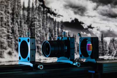 |
| Image sensor based on organic photodiodes on silicon in typical camera application. Background: NIR image. (Image: Fraunhofer FEP, Photographer: Jürgen Lösel)
|
|
Conventional silicon-based CMOS imagers are limited to a restricted wavelength region for fundamental technological reasons. They are usually set to the visible segment of the spectrum. If you want to detect light in the near-infrared (NIR), however, hybrid solutions such as combinations of indium gallium arsenide (InGaAs) with CMOS are usually resorted to.
|
|
Nevertheless, the manufacture of these kinds of hybrid solutions is considerably more costly and more prone to defects than fabrication using standard CMOS processes. This is where organic photodiodes offer an alternative. The organic layers can be integrated simply at wafer level and are therefore economical. Simultaneously, they also may have high sensitivity outside the visible wavelength region, depending on the system of materials selected.
|
|
The Fraunhofer FEP has extensive experience in integrating organic layers on CMOS wafers. Diverse OLED microdisplays (high-resolution, low power, embedded image sensors, ...) as well as sensors for fingerprint, flow, and photoelectric sensing applications have already been developed and fabricated.
|
|
“We will be debuting an organic photodiode array with SVGA resolution at SEMI European Imaging & Sensors Summit 2017. That means 800 × 600 pixels available for detection applications”, explains Philipp Wartenberg, head of the IC and System Design department at Fraunhofer FEP. “We have demonstrated that it is fundamentally feasible to fabricate a high-resolution organic photodiode matrix at this order of magnitude. It is sensitive at wavelengths up to 1,000 nanometers. We are able to develop customer- and application-specific organic photodiodes with optimized properties for the concrete application through appropriate adaption of material.”
|
|
The demonstrated image sensors were fabricated completely at wafer-level and therefore already under near-production conditions. With its extended region of sensitivity, the imager can be employed over the entire bandwidth of conventional applications in industry, automobiles, and medicine. They could be used for quality control of foodstuffs, as fingerprint sensors, and in biomedical tests, for example.
|
|
The scientists are now making the new technology available to industrial partners in order to jointly develop and produce optimized organic photodiodes and arrays as image sensors for their respective applications.
|

