| Posted: Sep 08, 2017 |
Integrated lasers on different surfaces
(Nanowerk News) Fabricating hybrid semiconductor lasers on materials other than the commonly used silicon-on-insulator (SOI) substrates has proved challenging. Now, A*STAR researchers have developed an innovative technique that can integrate the lasers on to a range of different materials (IEEE Journal of Selected Topics in Quantum Electronics, "Generic heterogeneously integrated III–V lasers-on-chip with metal-coated etched-mirror").
|
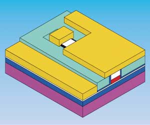 |
| Schematic of the hybrid laser. (Image: A*STAR Data Storage Institute)
|
|
Hybrid lasers combine the light-emitting properties of group III-V semiconductors like gallium arsenide and indium phosphide, with conventional silicon technologies, offering inexpensive photonic and microelectronic devices for application in optical telecommunication systems.
|
|
Their range of applications, however, is limited by the poor light-emitting characteristics of the silicon-on-insulator (SOI) wafers mostly used as substrates in the fabrication process. This spurred Doris Keh-Ting Ng and colleagues from the A*STAR Data Storage Institute to develop an innovative technique for bonding III-V lasers on to other substrates, be it silicon, quartz, or metal alloys.
|
|
By using an ultrathin layer of silicon oxide to bond the lasers to a silicon substrate, the researchers developed a simpler, safer and more flexible technique than direct bonding, which relies on chemical bonding between the surfaces.
|
|
“The challenge is to produce a smooth, extremely thin layer of silicon oxide on the surface of the substrate,” explains Ng. “By growing the film on the silicon substrate, but not on the III-V substrate, we greatly reduced the complexity of the process and improved the strength of the bond between the two materials.”
|
|
After first cleaning the surfaces with an organic solvent, the researchers exposed the surface to an oxygen plasma to increase its adhesive properties. They then initiated the bonding process at ambient temperature by bringing the two substrates slowly together, to reduce the air trapped between them, ensuring a much stronger bond.
|
|
The bonding was then completed at relatively low temperatures of around 220 degrees Celsius, allowing the ultrathin layer of silicon oxide to conduct heat between the layers, reducing potential damage to the materials, strengthening the bond and avoiding the need for hazardous chemicals, such as Piranha solution and hydrofluoric acid, used in direct bonding.
|
|
The work demonstrates a versatile on-chip laser that can be integrated on to any material platform and could lead to new applications for photonic devices, such as detector-on-chip and modulator-on-chip technologies.
|
|
“The low temperature interlayer approach is simpler and much safer than direct bonding, and means that laser manufacturers are not restricted by the choice of substrate,” says Ng.
|

