| Posted: Sep 28, 2017 |
A flexible new platform for high-performance electronics
(Nanowerk News) A team of University of Wisconsin–Madison engineers has created the most functional flexible transistor in the world — and with it, a fast, simple and inexpensive fabrication process that’s easily scalable to the commercial level.
|
|
It’s an advance that could open the door to an increasingly interconnected world, enabling manufacturers to add “smart,” wireless capabilities to any number of large or small products or objects — like wearable sensors and computers for people and animals — that curve, bend, stretch and move.
|
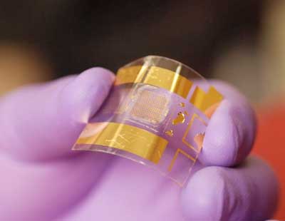 |
| Literal flexibility may bring the power of a new transistor developed at UW–Madison to digital devices that bend and move. (Image: Jung-Hun Seo, University at Buffalo, State University of New York)
|
|
Transistors are ubiquitous building blocks of modern electronics. The UW–Madison group’s advance is a twist on a two-decade-old industry standard: a BiCMOS (bipolar complementary metal oxide semiconductor) thin-film transistor, which combines two very different technologies — and speed, high current and low power dissipation in the form of heat and wasted energy — all on one surface.
|
|
As a result, these “mixed-signal” devices (with both analog and digital capabilities) deliver both brains and brawn and are the chip of choice for many of today’s portable electronic devices, including cellphones.
|
|
“The industry standard is very good,” says Zhenqiang (Jack) Ma, the Lynn H. Matthias Professor and Vilas Distinguished Achievement Professor in electrical and computer engineering at UW-Madison. “Now we can do the same things with our transistor — but it can bend.”
|
|
Ma is a world leader in high-frequency flexible electronics. He and his collaborators described their advance in the inaugural issue of the journal Flexible Electronics.
|
|
Making traditional BiCMOS flexible electronics is difficult, in part because the process takes several months and requires a multitude of delicate, high-temperature steps. Even a minor variation in temperature at any point could ruin all of the previous steps.
|
|
Ma and his collaborators fabricated their flexible electronics on a single-crystal silicon nanomembrane on a single bendable piece of plastic. The secret to their success is their unique process, which eliminates many steps and slashes both the time and cost of fabricating the transistors.
|
|
“In industry, they need to finish these in three months,” he says. “We finished it in a week.”
|
|
He says his group’s much simpler high-temperature process can scale to industry-level production right away.
|
|
“The key is that parameters are important,” he says. “One high-temperature step fixes everything — like glue. Now, we have more powerful mixed-signal tools. Basically, the idea is for flexible electronics to expand with this. The platform is getting bigger.”
|

