| Posted: Oct 03, 2017 |
Drawing at the one-nanometer length scale(Nanowerk News) At the Center for Functional Nanomaterials (CFN), scientists adapted a state-of-the-art electron microscope to carve structures at the single molecule level. This technique achieves unprecedented 1-nanometer resolution (Nano Letters, "Aberration-corrected electron beam lithography at the one nanometer length scale"). |
| The results are a significant improvement. The widely used nanofabrication technique, electron-beam lithography, could not achieve such details. |
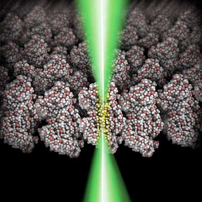 |
| A schematic showing a focused electron beam (green) shining through a polymeric film (grey: carbon atoms; red: oxygen atoms; white: hydrogen atoms). The glowing area (yellow) indicates the molecular volume chemically modified by the focused electron beam. (Image: Center for Functional Nanomaterials at Brookhaven National Laboratory) |
| With CFN’s approach, scientists can manipulate individual molecules to create a film with altered properties. For example, they could make films conduct electricity more efficiently. With this technique, scientists can fabricate a broad set of new materials, carved with arbitrary shapes. Scientists could build the materials with near atomic-scale control. |
| The ability to pattern materials at ever-smaller sizes — using electron-beam lithography, in which an electron-sensitive material is exposed to a focused beam of electrons — is driving advances in nanotechnology. When the feature size of materials is reduced from the macroscale to the nanoscale, individual atoms and molecules can be manipulated to dramatically alter material properties, such as color, chemical reactivity, electrical conductivity and light interactions. |
| In the ongoing quest to pattern materials with ever-smaller feature sizes, scientists at the Center for Functional Nanomaterials (CFN) — a U.S. Department of Energy Office of Science user facility at Brookhaven National Laboratory — have recently set a new record. |
| Performing electron-beam lithography with a state-of-the-art scanning transmission electron microscope, they have patterned thin films of the polymer poly(methyl methacrylate) (PMMA) with individual features as small as 1 nanometer, and with a spacing between features of 11 nm, yielding an areal density of nearly 1 trillion features per square centimeter. |
| The team’s patterned PMMA films can be used as stencils for transferring the drawn single-digit nanometer feature into any other material. In this work, the scientists created structures smaller than 5 nanometers in both metallic (gold palladium) and semiconducting (zinc oxide) materials. Their fabricated gold palladium alloy features were as small as 6 atoms wide. |
| This technique opens up many exciting materials engineering possibilities, tailoring properties closer to the atomic scale. The CFN will soon be offering this first-of-a-kind nanoscience tool to users from around the world. |
| Source: U.S. Department of Energy, Office of Science |

